Bipolar Switch Hall-Effect ICs
There are four general categories of Hall-effect IC devices that provide a digital output: unipolar switches, bipolar switches, omnipolar switches, and latches. Bipolar switches are described in this application note. Similar application notes on unipolar switches, omnipolar switches, and latches are provided on the Allegro™ website.
Bipolar sensor ICs are designed to be sensitive switches. (Note that the term "bipolar" refers to magnetic polarities, and is not related to bipolar semiconductor chip structures.) A bipolar switch has consistent hysteresis, but individual units have switchpoints that occur in either relatively more positive or more negative ranges. These devices find application where closely-spaced, alternating north and south poles are used, resulting in minimal required magnetic signal amplitude, ΔB, because the alternation of magnetic field polarity ensures switching, and the consistent hysteresis ensures periodicity.
Applications for detecting the position of a rotating shaft, such as in a brushless dc motor (BLDC) are shown in figure 1. The multiple magnets are incorporated into a simple structure referred to as a "ring magnet," which incorporates alternating zones of opposing magnetic polarity. The IC package adjacent to each ring magnet is the Hall bipolar switch device. When the shaft rotates, the magnetic zones are moved past the Hall device. The device is subjected to the nearest magnetic field and is turned-on when a south field is opposite, and turned-off when a north field is opposite. Note that the branded face of the device is toward the ring magnet.
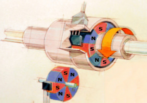
Figure 1. Two bipolar device applications using ring magnets. The ring magnets have alternating N (north) and S (south) polarity zones, which are rotated past the Hall devices, causing them to turn on and off.
Magnetic Switchpoint Terms
The following are terms used to define the transition points, or switchpoints, of Hall switch operation:
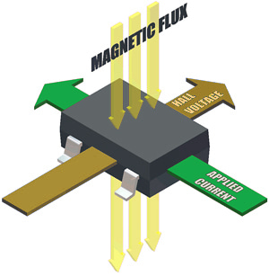
Figure 2. The Hall effect refers to the measurable voltage present when an applied current is influenced by a perpendicular magnetic field.
- B − The symbol for Magnetic Flux Density, the property of a magnetic field used to determine Hall device switchpoints. Measured in gauss (G) or tesla (T). The conversion is 1 G = 0.1 mT.
B can have a north or south polarity, so it is useful to keep in mind the algebraic convention, by which B is indicated as a negative value for north-polarity magnetic fields, and as a positive value for south-polarity magnetic fields. This convention allows arithmetic comparison of north and south polarity values, where the relative strength of the field is indicated by the absolute value of B, and the sign indicates the polarity of the field. For example, a − 100 G (north) field and a 100 G (south) field have equivalent strength, but opposite polarity. In the same way, a − 100 G field is stronger than a − 50 G field.
- BOP − Magnetic operate point; the level of a strengthening magnetic field at which a Hall device switches on. The resulting state of the device output depends on the individual device electronic design.
- BRP − Magnetic release point; the level of a weakening magnetic field at which a Hall device switches off (or for some types of Hall devices, the level of a strengthening negative field given a positive BOP). The resulting state of the device output depends on the individual device electronic design.
- BHYS − Magnetic switchpoint hysteresis. The transfer function of a Hall device is designed with this offset between the switchpoints to filter out small fluctuations in the magnetic field that can result from mechanical vibration or electromagnetic noise in the application. BHYS = | BOP − BRP |.
Typical Operation
Bipolar switches usually have a positive BOP and negative BRP, but these switchpoints occur at field strength levels that are not precisely symmetrical with respect to the neutral level, B = 0 G. This characteristic is allowed so bipolar switches can provide greater sensitivity and narrower BHYS than latching switches (bipolar switches were originally conceived as a lower-cost alternative to early latches). A small percentage (≈10%) of bipolar switches have switchpoint ranges entirely in the positive (south) polarity range or entirely in the negative (north) polarity range. All of these characteristic ranges can be reliably operated using alternating positive (south) and negative (north) polarity fields. Turn-off will usually occur when the magnetic field is removed, but to ensure release, a field reversal is required.
An example of a bipolar switch would be a device with a maximum operate point, BOP(max), of 45 G, a minimum release point, BRP(min), of –40 G, and a minimum hysteresis, BHYS(min), of 15 G. However, the minimum operate point, BOP(min), could be as low as –25 G, and the maximum release point, BRP(max), could be as high as 30 G. Figure 3 shows these characteristics for units of a hypothetical device with those switchpoints. At the top of figure 3, trace "Minimum ΔB" demonstrates how small an amplitude can result in reliable switching.
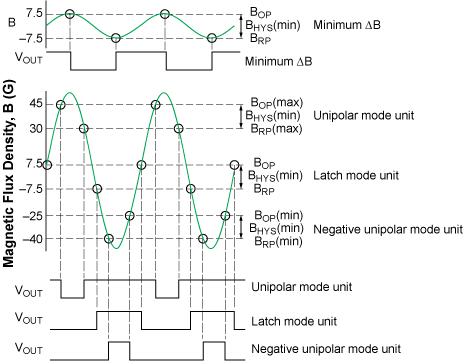
Figure 3. Demonstration of possible switchpoint ranges for a bipolar switch, for use with low magnetic flux amplitude, narrow pitch alternating pole targets
Figure 3 illustrates the variances between the three general operating modes of bipolar switches:
- "latch mode" describes any bipolar switch unit with a positive BOP and negative BRP, behaving like a Hall latching switch by requiring both magnetic fields to be present for complete operation (but without actual latching of the device state)
- "unipolar mode" describes any bipolar switch unit with both BOP and BRP in the positive (south) range
- "negative unipolar mode" (sometimes referred to as "negative switch" mode) describes any bipolar switch unit with both BOP and BRP in the negative (north) range
The release point flux density becomes less important because, if the Hall switch has not switched when the pole has passed and the flux density approaches the neutral level, B = 0 G, the switch will certainly turn off when the following pole increases the flux density in the opposite polarity. Bipolar Hall switches take advantage of this extra margin in release-point flux values to achieve lower operate-point flux densities, a definite advantage in ring magnet applications.
As can be seen in the VOUT traces at the bottom of figure 3, for each of these modes, switching at each pole alternation is reliable, with the duty cycle of the output differing somewhat according to the operating mode. A bipolar device operating in latch mode has nearly symmetrical switchpoints. This tends to set the duty cycle to near perfection when working with equally-spaced ring magnet poles. Having said that, even if the switchpoints were skewed, the duty cycle will still be close to 50% on and 50% off. For motor commutation this is ideal, resulting in high efficiency. Units having unipolar mode turn on and off with the south pole and do nothing as the north pole passes. Units in this mode will have a duty cycle of perhaps 40% on and 60% off. Units in negative unipolar mode turn off and on with the north pole and do nothing as the south pole passes. Units in this mode will have a duty cycle of perhaps 60% on and 40% off.
The three panels of figure 4 show the transfer characteristics of the operating modes of bipolar sensor ICs.
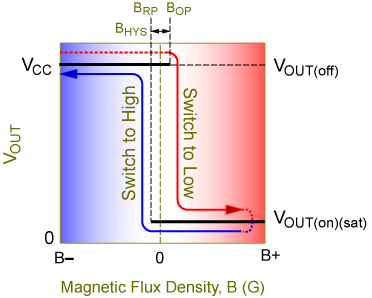
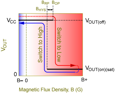
Figure 4A. Latch mode characteristic. Note that the switchpoint hysteresis zone, BHYS, includes the neutral flux density level, B = 0 G.
- For purposes of explanation of figure 4A, assume the device powers-on with the magnetic flux density at the far left, where the magnetic flux (B, on the horizontal axis) is more negative than BRP or BOP. Here the device is off, and the output voltage (VOUT, on the vertical axis) is high.
- Following the arrows toward the right, the magnetic field becomes increasingly positive. When the field is more positive than BOP, the device turns on. This causes the output voltage to change to the opposite state, low.
- While the magnetic field remains more positive than BRP, the device remains turned-on, and the output state remains unchanged. This is true even if B becomes slightly less positive than BOP, within the built-in zone of switching hysteresis, BHYS.
- Following the arrows back toward the left, the magnetic field becomes less positive and then more negative. When the magnetic field again drops below BRP, the device turns off. This causes the output to change back to the original state, high.
- For purposes of explanation of figure 4B, assume the device powers-on with the magnetic flux density at the far left, where the magnetic flux (B, on the horizontal axis) is less positive than BRP or BOP. Here the device is off, and the output voltage (VOUT, on the vertical axis) is high.
- Following the arrows toward the right, the magnetic field becomes increasingly positive. When the field is more positive than BOP, the device turns on. This causes the output voltage to change to the opposite state, low.
- While the magnetic field remains more positive than BRP, the device remains turned-on, and the output state remains unchanged. This is true even if B becomes slightly less positive than BOP, within the built-in zone of switching hysteresis, BHYS.
- Following the arrows back toward the left, the magnetic field becomes less positive. When the magnetic field again drops below BRP, the device turns off. This causes the output to change back to the original state, high.
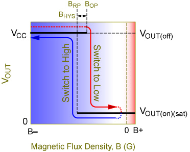
Figure 4C. Negative unipolar (negative switch) mode characteristic. Note that the switchpoint hysteresis zone, BHYS, is entirely more magnetically north than the neutral flux density level, B = 0 G. A south magnetic field has no effect on the device, although it can aid switching by dissipating any flux remaining after a north field has passed.
- For purposes of explanation of figure 4C, assume the device powers-on with the magnetic flux density at the far left, where the magnetic flux (B, on the horizontal axis) is more negative than BRP or BOP. Here the device is off, and the output voltage (VOUT, on the vertical axis) is high.
- Following the arrows toward the right, the magnetic field becomes less negative. When the field is less negative than BOP, the device turns on. This causes the output voltage to change to the opposite state, low.
- While the magnetic field remains less negative than BOP, the device remains turned-on, and the output state remains unchanged. This is true even if B becomes slightly less positive than BOP, within the built-in zone of switching hysteresis, BHYS.
- Following the arrows back toward the left, the magnetic field becomes less positive. When the magnetic field again drops below BRP, the device turns off. This causes the output to change back to the original state, high.
Magnets
Individual magnets may be used to provide the two opposing magnetic polarities, however, it is usually more cost effective to use ring or strip magnet material. Ring and strip magnets are magnetized with alternating poles with specified spacing. A ring magnet is a toroid- or disc-shaped assembly (see figure 1) with alternating radially- or axially-magnetized poles. A strip magnet is a flat strip with alternating magnetic poles. Ring magnets are available in a variety of materials including ceramic, rare earth, and flexible materials. Strip magnets nearly always utilize flexible materials such as Nitrile rubber binder containing oriented barium ferrite, or higher energy rare-earth materials.
Ring magnets normally are specified as having a number of poles while strip magnets are normally specified in poles-per-inch. A four-pole ring magnet contains two north and two south oriented alternating poles (N-S-N-S) while an 11 pole-per-inch strip magnet has alternating poles spaced on 0.0909-in. centers. A variety of pole spacings are available from magnet manufacturers.
Pull-Up Resistor
A pull-up resistor must be connected between the positive supply and the output pin (see figure 4). Common values for pull-up resistors are 1 to 10 kΩ. The minimum pull-up resistance is a function of the sensor IC maximum output current (sink current) and the actual supply voltage. 20 mA is a typical maximum output current, and in that case the minimum pull-up would be VCC / 0.020 A. In cases where current consumption is a concern, the pull-up resistance could be as large as 50 to 100 kΩ. Caution: With large pull-up values it is possible to invite external leakage currents to ground, which are high enough to drop the output voltage even when the device is magnetically off. This is not a device problem but is rather a leakage that occurs in the conductors between the pull-up resistor and the sensor ICs output pin. Taken to the extreme, this can drop the sensor IC output voltage enough to inhibit proper external logic function.
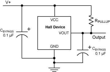
Figure 5. Typical application diagram.
Use of Bypass Capacitors
Refer to figure 5 for a layout of bypass capacitors. In general:
- For designs without chopper stabilization − It is recommended that a 0.01 µF capacitor be placed the output and ground pins and between the supply and ground pins.
- For designs with chopper stabilization − A 0.1 µF capacitor must be placed between the supply and ground pins, and a 0.01 µF capacitor is recommended between the output and ground pins.
Power-On State
A bipolar device powers-on in a valid state only if the magnetic field strength either exceeds BOP or is less than BRP when power is applied. If the magnetic field strength is in the hysteresis band, that is between BOP and BRP, the device can assume either an on or off state initially, and then attains the correct state at the first excursion beyond a switchpoint. Devices can be designed with power-on logic that sets the device off until a switchpoint is reached.
| Power-On States | |
|---|---|
| Sensor IC Type | Power-On State (0 G Field) |
| Unipolar Switch | Off |
| Latch | Either state1,2 |
| Negative Switch | On2 |
| 1Unless power-on logic is incorporated in the design. 2Unless power-on of the device occurs while the magnetic field is inside the specified magnetic hysteresis of the device. |
|
Power-On Time
Power-on time depends to some extent on the device design. Digital output sensor ICs, such as the bipolar device, reach stability on initial power-on in the following times.
| Device type | Power-on time |
|---|---|
| Non-chopped designs | <4 µs |
| Chopper-stabilized | <25 µs |
Basically, this means that prior to this elapsed time after providing power, device output may not be in the correct state, but after this time has elapsed, device output is guaranteed to be in the correct state.
Power Dissipation
Total power dissipation is the sum of two factors:
- Power consumed by the sensor IC, excluding power dissipated in the output. This value is VCC times the supply current. VCC is the device supply voltage and the supply current is specified on the datasheet. For example, given VCC = 12 V and Supply current = 9 mA. Power dissipation = 12 × 0.009 or 108 mW.
- Power consumed in the output transistor. This value is V(on)(sat) times the output current (set by the pull-up resistor). If V(on)(sat) is 0.4 V (worst case) and the output current is 20 mA (often worst case), the power dissipated is 0.4 × 0.02 = 8 mW. As you can see, because of the very low saturation voltage the power dissipated in the output is not a huge concern.
Total power dissipation for this example is 108 + 8 = 116 mW. Take this number to the derating chart in the datasheet for the package in question and check to see if the maximum allowable operational temperature must be reduced.
Frequently Asked Questions
Q: How do I orient the magnets?
A: The magnet poles are oriented towards the branded face of the device. The branded face is where you will find the identification markings of the device, such as partial part number or date code.
Q: Can I approach the device back side with the magnet?
A: Yes, however bear this in mind: if the poles of the magnet remain oriented in the same direction, then the orientation of the flux field through the device remains unchanged from the front-side approach (for example, if the south pole was nearer the device in the front-side approach, then the north pole would be nearer the device in the back-side approach). The north pole would then generate a positive field relative to the Hall element, while the south pole would generate a negative field.
Q: Are there trade-offs to approaching the device back side?
A: Yes. A "cleaner" signal is available when approaching from the package front side, because the Hall element is located closer to the front side (the package branded face) than to the back side. For example, for the "UA" package, the chip with the Hall element is 0.50 mm inside the branded face of the package, and so approximately 1.02 mm from the back-side face. (The distance from the branded face to the Hall element is referred to as the "active area depth.")
Q: Can a very large field damage a Hall-effect device?
A: No. A very large field will not damage an Allegro Hall-effect device nor will such a field add additional hysteresis (other than the designed hysteresis).
Q: Why would I want a chopper-stabilized device?
A: Chopper-stabilized sensor ICs allow greater sensitivity with more-tightly controlled switchpoints than non-chopped designs. This may also allow higher operational temperatures. Most new device designs utilize a chopped Hall element.
Suggested Devices
Allegro bipolar switches are listed in the selection guides on the company website, at Hall-Effect Latches and Bipolar Switches.
Possible Applications
- Brushless dc motor rotation
- Speed sensing
- Pulse counters, encoders
- Automotive
Application Notes on Related Device Types
Reference: AN27705