Soldering Methods for Allegro Products (SMD and Through-Hole)
By Bradley Smith and John Sauber
Allegro MicroSystems, LLC
SCOPE
This document describes typical soldering methods that have been proven effective with Allegro products. It provides information on SMD (surface mount devices) and through-hole packages. Both lead (Pb) free and traditional Pb-based technologies are examined.
AVAILABLE STANDARDS
Allegro recommends becoming familiar with IPC/JEDEC Joint Industry Standard J-STD-020, Moisture/Reflow Sensitivity Classification for Nonhermetic Solid State Surface Mount Devices. It provides information on MSL (moisture sensitivity level) classifications for devices, and the corresponding protocols for device handling. In addition, important information on determining optimum soldering process parameters can be found in J-STD-002, Solderability Tests for Component Leads, Terminations, Lugs, Terminals and Wires.
The characterization of an acceptable solder joint can be somewhat different between Pb-based and Pb-free technologies. The IPC has several publications and course materials that provide information on solder joint evaluation. A primary source is IPC J-STD-001, Requirements for Soldered Electrical and Electronic Assemblies, which is an industry-level consensus standard covering soldering materials and processes, with revision G and later including coverage of Pb-free soldering. IPC-A-610, Acceptability of Electronic Assemblies, provides detailed workmanship
standards, with revision G and later including coverage of Pb-free processes. Training courses and certification for IPC-A-610 should be used by all customers performing soldering operations. By becoming certified, customers will have the knowledge to evaluate the solder joints for acceptability to international standards.
IPC-2221, Generic Standard on Printed Board Design, provides a notation for dimensioning joints.
Parallel bodies of standards and information are available from the IEC (International Electrotechnical Commission), which is a particularly good source for international and European standards, and from JEITA (Japan).
PROCESS TEMPERATURE AND MSLS
A significant process concern is the absorption of atmospheric moisture by devices before exposure to elevated soldering temperatures such as reflow oven soldering.
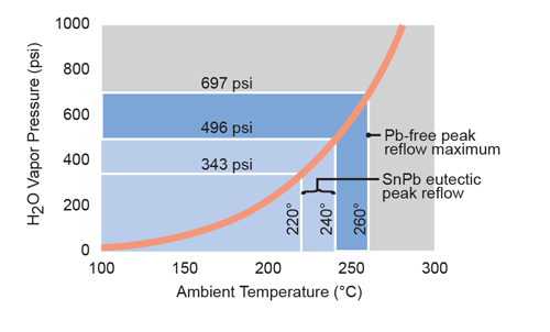
The device packages commonly used throughout the industry, including by Allegro, are nonhermetic. The package body is composed of plastic epoxy molding compounds that can absorb moisture and other contaminants. Expo- sure to atmospheric moisture over even short periods of time can allow enough moisture to be absorbed to have serious effects when the moisture turns to steam during reflow oven heating. As shown in Figure 1, vapor pressure increases rapidly as temperature increases, resulting in a disproportionate increase in pressure for the comparatively small increments of process temperature between the different process types. From a Pb-based process peak of about 220°C (493 K), to the Pb-free lower range in the vicinity of 240°C (513 K), is an increase of approximately 4% in temperature, but 45% in vapor pressure. The transi- tion from Pb-based to the maximum limit of 260°C (533 K) involves a temperature increase of only about 8%, but the vapor pressure increase is approximately 103%.
To avoid delamination from vaporization effects, take care to avoid exceeding the maximum floor life of the devices. In this context, floor life is linked to the rate at which the device absorbs atmospheric moisture, represented by the MSL rating (moisture sensitivity level) at the rated reflow temperature (if not stated, is assumed to be 260°C). If the MSL level states a different reflow temperature, such as MSL 3 at 250°C, the open bag shelf life is one week with a maximum reflow temperature of 250°C. If a cus- tomer is using a reflow temperature below the maximum rating, such as 240°C, the MSL level will be better. Thus, if a device package has a 260°C MSL 3 rating but if the customer reflow temperature is 240°C, the MSL rating at that temperature may be MSL 2 (check with Allegro if there is data for that package). Note that all Allegro devices are qualified for 3 passes of reflow. Reflow profiles are not specified by Allegro; it is up to the customer to produce the proper profile based upon their parts, board, and reflow oven type. The peak reflow temperature and MSL level does need to be adhered to.
- MSL 1 is the most resistant to delamination, with a shelf life in an opened bag of unlimited time (at <30°C/85%RH).
- MSL 2 is one-year shelf life in an open bag (at <30°C/60%RH).
- MSL 3 is one-week shelf life in an open bag (at <30C/60%RH).
Protocols for rating moisture absorption, as well as absorption abatement, are provided in J-STD-020, revisions E and later. Information on the MSL rating is provided in the labeling on the device packing labels. MSL ratings are linked to the peak reflow temperature, as stated on the label.
Devices can also be sensitive to just heat alone and a rating for this is the PSL (process sensitivity level) [J-STD- 075]. This can also be printed on the shipping label.
TERMINAL FINISHES
Finish Appearance
Pb-free finishes and resulting solder joints tend to be inherently less bright and reflective compared to those of Pb-based finishes. Specifically, 100% matte tin plating is commonly used for terminal finishes. This does not affect solder joint integrity, and is recognized in IPC J-STD-001, as a characteristic of materials and processes:
“There are solder alloy compositions, component lead and terminal finishes… and special soldering processes… that may produce dull, matte, gray, or grainy appearing solders that are normal… these solder joints are acceptable.”
“The primary difference between the solder connections created with processes using tin-lead alloys and processes using lead free alloys is related to the visual appearance of the solder. All other solder fillet criteria are the same… Lead-free and tin-lead connections may exhibit similar appearances, but lead-free alloys are more likely to have surface roughness (grainy or dull) or different wetting contact angles.” (Rev. D, §4.14).
This characteristic is exacerbated by use of higher temperatures during manufacturing, testing, bake-out, and soldering. Allegro devices are subjected to more testing than is common in the industry. This ensures high reliability for the device but may cause terminal platings to appear dull or tarnished. Another source of dulling is exposure to atmospheric conditions during long-term storage of devices before soldering into an assembly. Such appearance factors are not significant to the integrity of the solder joint because they are superficial.
Automatic optical inspection equipment may have to be adjusted to offset the lower illumination returned by matte tin plating. This can help to prevent rejection of devices that in fact have proper finish and joints that have been properly formed. Unless optical inspection equipment is tuned to device terminals and joints with duller finishes, usable devices and assemblies may be unnecessarily rejected or reworked.
Finish Coverage
The finish that is plated over the base metal core of the leadframe protects the copper core and performs a vital role in the effectiveness of the solder joint, by providing a surface that is easily wetted by the solder.
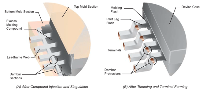
Three primary process factors affect how the plating on exposed leads and contacts cover and provide a wetting surface for solder: molding flash, mechanical wear, and oxidation due to singulation.
Molding Flash. Plating can be applied to terminals prior to or after molding. Pre-plated leadframes are composed of nickel/palladium/gold. Plating after molding is 100% matte tin.
During molding, the leadframe and die assembly are enclosed from above and below by the mold halves. The mold halves remain separated by the leadframe, as shown in Figure 2.
When the molding compound is injected forcibly into the mold cavity, excess compound extrudes through the gaps between the terminals, and smaller amounts seep between the mold halves and the upper and lower surfaces of the terminals. A residual amount of excess molding compound—referred to as pant-leg flash—can remain along the sides of the terminals, between the case, and where the dambar sections were located. In addition, a small amount of flash may remain along the top and bottom surfaces of the terminal, near the case.
Mechanically trimming all the residual flash could result in abrasion of the case, terminal finish, and the terminal copper base material. When the terminal is plated after package molding, no plating occurs where there is flash. The residual flash that is not removed is remote from the critical soldering areas of the terminal and does not affect solder joint strength. Exposed copper areas on the leads are a necessary part of the assembly process and are not required to be soldered.
Abrasion During Handling. Terminal finish may be reduced by wear from handling after plating. Experience has shown that Pb-free devices frequently undergo additional test and evaluation cycles, which occur at elevated process temperatures. Such additional process- ing exposes these devices to removal of terminal finish by mechanical abrasion. For example, movement of devices though tracks while resting on terminals erodes the finish on the underside of the terminal contact area. This abrasion is normal and does not impact the wetting of the terminal during soldering.
A side effect of increased abrasion is an increased risk of adhesion of debris and particulates worn from previously processed devices. If extremely excessive contamination is present and the leads are blackened, this may affect solderability and require a stronger flux to be used. To help prevent this contamination, procedures must be qualified for routine and thorough cleaning of feed bowls, tracks, output bins, and carriers used for handling devices.
Singulation. In this process stage, the individual device packages are separated from the larger leadframe web that contains them during the various manufacturing stages. Additional lead forming and trimming may take place post-production or at the site where the device is assembled into the end-product.
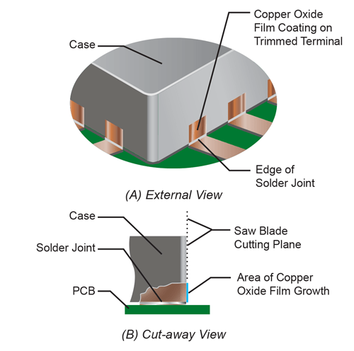
As shown in Figure 2, where the terminals are trimmed at their ends and where the dambar sections have been removed, the core copper is exposed. These exposed areas are away from the soldering critical areas. Figure 3 shows the results of singulation on QFNs and SONs. In those packages, the molding compound is a continuous block, and the individual devices are sawn out of the block. As a result, the exposed copper of the terminal ends appears in the same plane as the case wall. In some designs, the terminal does not extend as far as the saw plane, and there are no exposed copper areas on the terminals.
Where the core copper is exposed, a film of copper oxides forms eventually. This prevents wetting by the solder, except under conditions of very active flux. Soldering over exposed copper base material is not guaranteed and is not required for joint integrity by standards such as IPC J-STD-001 or IPC A-610. For QFNs and SONs, in fact, optical inspection methods cannot be used in production, because there is characteristically no fillet formed, as the critical area of soldering between the device contacts and the solder pad lies completely beneath the package. Electrical or x-ray testing and inspection methods must be used instead.
Allegro does have some packages with a wettable flank that does form a visible fillet on QFNs.
Allegro Pb-Free Finish
The standard finish used by Allegro on its Pb-free devices is 100% matte tin plating. This finish has gained acceptance in the marketplace. It provides a robust solder joint when device terminals and solder lands are properly aligned and common solder reflow profiles are followed. It has workable wear characteristics and does not use expensive noble metals as constituents.
Another advantage of matte tin finish is 100% backward- compatibility with traditional tin-lead (SnPb) solders of any composition. It can be soldered at any temperature that has been traditionally used for SnPb solder alloys. Thus, Allegro devices with 100% matte tin leadframe plating can be used in existing SnPb processes, includ- ing processes that peak below 232°C, the melting point of tin. This is because the matte tin dissolves easily into molten SnPb solder.
Shelf Life for Solderability
Allegro parts with 100% matte-tin-plated or pre-plated metals are resistant to oxidation or other degradation that might affect solderability. Refer to application note: AN296126, Handling, Storage, and Shelf Life of Semi- conductor Devices.
SOLDERS AND FLUXES
An appropriate combination of solder and flux must be used for soldering devices to PCBs. Optimum combina- tions account for the leadframe finish of the device, as well as the PCB condition, process chemistry, and placement equipment characteristics.
Flux Alternatives
Allegro strongly recommends that experiments be conducted with several combinations of fluxes, solders, and terminal finishes. Fluxes and solder pastes must be properly stored and handled, according to manufacturer instructions. A series of assembly process combinations using different fluxes and conditions should be qualified, which can then be available to accommodate variances in device finishes and reflow temperature requirements.
An important reason for experimenting with alternative fluxes is that using more highly activated solders can avoid adjustments to other process factors that can be more expensive or sensitive. Increasing process temperatures can improve solderability but forcing temperatures too high can generate complications with materials. Further, in Pb-free processes, the headroom for raising tempera- tures is limited because the baseline temperatures are already elevated.
Another process adjustment that can improve solderability is increasing the proportion of nitrogen in the atmosphere of the solder chamber. Newer processing equipment is equipped to support controlled atmospheres in process chambers. Allegro recommends use of nitrogen-enriched, controlled atmospheres in reflow soldering operations, particularly for Pb-free operations.
Regarding solderability, there are three basic classes of fluxes:
- aqueous-clean fluxes
- no-clean
- solvent-clean
Allegro highly recommends halide-free aqueous-clean fluxes because of their high activation levels. These also have the advantage of allowing surfactants for cleaning that are environmentally more benign than traditional solvent cleaning compounds. No-clean fluxes have an even greater environmental advantage but are not as highly activated as the aqueous-clean fluxes.
No-clean fluxes must be used if there is no 100% halide- free aqueous flux qualified (ensure that the no-clean flux itself has 0% halides). Both flux types leave less residue or residue that is more benign than rosin-core or fluxes that must be removed with solvents. Note that so-called no-clean fluxes must still be removed from the PCB board after soldering because the residue can still be harmful.
Allegro packages are compatible with all process chemistries, including all halide-free aqueous- or solvent-based flux cleaning processes except 1,1,1-trichloroethane and trichloroethylene, which have been shown to produce chlorides that can corrode the devices. Those solvents have also been demonstrated to contribute to atmospheric ozone depletion and should be avoided.
| Table 1. Comparison of Typical Solder Paste and Wave Solders |
||
|---|---|---|
| Common Name |
Typical Composition |
Comment |
| BiSn |
Bi 58% / Sn 42% |
Melting point 138°C; Not recommended–relatively weak joint strength when subject to temperature cycling; compatible with 100% matte tin finishes; not compatible with existing SnPb finishes |
| SnPb (Eutectic) |
Sn 60% / Pb 40% |
Melting point 183°C; common use for electronic applications; compatible with 100% matte tin finishes; shiny appearance |
| SAC305 |
Sn 96.5% / Ag 3.0% / Cu 0.5% |
Melting point 219°C; compatible with existing SnPb finishes and 100% matte tin finishes; dull appearance |
| SnAg |
Sn 96.5% / Ag 3.5% |
Melting point 221°C; compatible with 100% matte tin finishes; not compatible with existing SnPb finishes |
| SnCu |
Sn 99.3% / Cu 0.5 % |
Melting point 227°C; compatible with existing SnPb finishes and 100% matte tin finishes; dull appearance |
| SN100 |
Sn >98% / Cu <1.0% / Ni <1.0% |
Melting point 232°C; compatible with existing SnPb finishes and 100% matte tin finishes; shiny appearance |
| SnPb(High-Temperature) |
Sn 5% / Pb 95% |
Melting point ≈ 300°C, common use for flip-chip and similar applications; compatible with 100% matte tin finishes and existing SnPb finishes |
Alternative Solder Types
Table 1 provides a basic comparison of a selection of Pb-free solder alloys.
Characteristics of materials and process chemistry integ- rity have become increasingly important with the stricter demands imposed by Pb-free processing. In general, Pb- free alloys have higher surface tensions and wet more slowly than Pb-based alloys, requiring more extensive preheating. This in turn places new demands on fluxes to remain active for longer periods of time, and to maintain their properties at elevated temperatures. Note that bismuth-containing solder cannot be used with any lead-containing system. Low temperature solders can be used with Allegro devices with 100% matte tin finish even though tin melts at 232°C because the tin dissolves in the low melting solder and forms a good joint.
CORROSIVE CONTAMINANTS
Major contributors to corrosion are halide compounds. Materials containing halides should be strictly avoided in the assembly process. This applies not only to fluxes but also to solders and solder pastes, and to overmolding com- pounds. Of concern are nylon overmolding compounds, which can be highly susceptible to moisture absorption and chloride can migrate through it.
The best defense against such corrosion is to eliminate halides from all materials used in the manufacturing process. For example, higher-grade nylons typically have minimal halide content. Such efforts should be supplemented by regular vetting of all process stages to ensure that no sources of contamination have been introduced. Sources can include not only materials consumed in manufacturing, but also substances that can be conveyed on the persons of production workers. Face masks, gloves, and suitable gowning should always be in use. So-called “halide free” solder pastes may only mean no halides have been purposely added and not that there is 0%.
ASSEMBLY CONSIDERATIONS
The interaction of the mechanical characteristics of the PCB, terminal, and solder joint also must receive renewed attention. A detailed discussion of soldering and other assembly methods is provided in the Allegro application note AN27703.1, Guidelines for Designing Subassemblies Using Hall-Effect Devices. The lowest peak reflow temperature (generally in the range 235°C to 245°C) that results in optimum soldering should be used.
Solder Wetting
According to IPC-JSTD-001, a good joint has the appear- ance of adhesion and wetting to all soldered surfaces, and the blend from the solder surface to the soldered terminal or land surface should be smooth, usually with an angle of less than 90 degrees (although exceptions are provided). (Rev. D, §4.14). IPC-JSTD-001 does not require that all terminal areas with surface finish be covered with solder (Rev. D, §4.14.2).
At areas of the terminal where the finish is not present, wetting may not occur, and solder adhesion cannot be guaranteed. A prime example is the extremity of a terminal, or of the dambar protrusions or intrusions, where trimming during singulation or device mounting leaves the core material of the terminal exposed. Another location of concern is the seating surface of the terminal, where the finish can be abraded by movement during handling. These areas are not cause for rejection or concern.
|
|
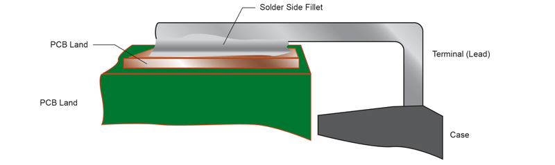
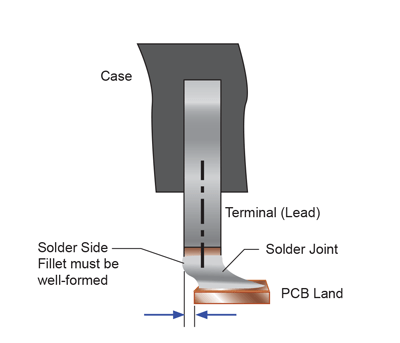
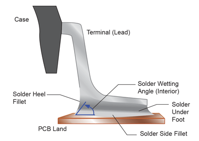
Fillet Shape
To promote well-formed solder fillets, lateral overlap of ter- minals and land areas by no less than 75% of the terminal width is required for high-reliability (IPC class 3) assembly, as shown in Figure 4. Regardless of the amount of over- hang, failure to form a solder side fillet on the overhung side of the terminal is a PCB alignment issue rather than an outcome of finish chemistry. Allegro strongly recommends as close to 100% alignment of the terminal width and foot with the PCB land pad. The formation of fully filleted solder joints is not guaranteed where terminal and lands do not completely align.
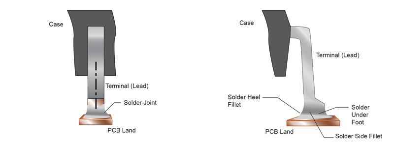
An acceptable solder joint is typically one in which there is a well-formed solder fillet on each of the two sides of the terminal: on the heel, and a solder layer under the terminal foot, as shown in Figure 5. In the standard JESD22, the Critical Area for gull-wing solder joints comprises the lateral sides of the terminal and the underside of the terminal, where it meets the land pad (§5.3.3.2, Accept/ Reject Criteria).
For detailed information on SMD solder joint evaluation, see IPC-A-610 §8; the IPC Desk Reference Manual for Surface Mount Solder Joint Evaluation also provides examples of target conditions and fillet shape acceptance criteria. For flat ribbon, L, and gull-wing terminals, such as those shown in the illustrations on the previous pages, solder thickness is considered adequate when a wetted fillet is evident between the solder and the terminal and PCB land (§8.2.5.7). The minimum length of the side fil- let is specified as the greater of either 3 times the width of the terminal or 75 % of the terminal foot length over the PCB land when the foot length is at least 3 times the width of the terminal(§8.2.5).
Regarding toe fillets, IPC provides for exposure of base material in trim areas of terminals (IPC J-STD-001, Rev. D, §4.14.1). Thus, fillets at the underside of the toe are expected, but fillets covering the entire toe may be more difficult to achieve where there is exposed copper and are not cause for rejection.
JESD22 does not include the top surface of a gull-wing terminal in consideration of the solder joint Critical Area (JEDEC figure 2). The top surface also is not included in the IPC-2221A solder joint description notation (IPC figure 8-16) or in the IPC J-STD-001 acceptability standards. Care is recommended to avoid excessive solder fillet height, to avoid contact with the device package body. When using exposed terminal designs, such as gull wing, optimized process conditions may be required to enable the solder to wick over the 90-degree edges of the top surface of the terminal and adhere to it. In general, greater quantities of more active fluxes are necessary to ensure solder coverage of the top surface of a gull-wing lead. Thus, the top surface of a terminal is not guaranteed to solder. Flow characteristics of solders should be evaluated to ensure proper filleting of the heel, toe, and side terminal joints.
Manual Soldering
Manual soldering of through-hole devices is acceptable if care is taken to prevent the package body from being exposed to excessive temperatures. In general, manual soldering of SMDs should be avoided because of the difficulty in controlling the preheating and cooling phases of the soldering procedure unless specialized equipment is used.
Hot air guns should not be used. Their effect can be difficult to control because they produce large volumes of heated air that can quickly damage plastic components and overspread the PCB, loosening the joints of adjacent components. Specialized hot air solder equipment is acceptable and is commonly used for spot rework or custom manufacturing.
If manual assembly is required (such as for prototype assembly or board rework), a soldering iron is preferred, in particular irons that are self-regulated and can be set to maintain a maximum temperature of under 350°C with a dwell time maximum of 7 seconds. An example is the Metcal SmartHeat®. The iron temperature should be set as low as possible without extending the soldering time. Only trained, experienced technicians should be allowed to perform the soldering. Parallel clamp soldering is also a good tool to use for certain applications.
Welding
Welding of copper-core terminals for Allegro devices that have long terminal lengths should be performed using a method that results in the lowest temperature (power setting) consistent with a good solder joint to minimize the spattering of the terminal finish. Notes are found in in the Allegro application note AN27703.1, Guidelines for Designing Subassemblies Using Hall-Effect Devices. Allegro reduces average terminal thickness to be more compatible with welding processes.
Allegro finishes have a mean thickness of approximately 450 μin., with a range of 300 to 800 μin., measured at the active area of the terminal on the seating plane. This thickness is considered optimal for processing because thicker finishes, on the order of 600 μin. or more, have a greater propensity to splatter, particularly at the elevated temperatures found in welding.
Optimum process temperatures should be determined experimentally, to ensure that the finish can be melted for proper bonding, without boiling and spattering. Welding at too high a temperature results in boiling away the finish from the terminals while bonding the copper of the terminal directly to the copper of the contact pad. This higher heat (red hot) oxidizes the weld head tip and can create poor welds or non-sticks. This is not the fault of the tin plating but too high weld current conditions.
Efforts must be made to shield surrounding areas from the spatter of the molten tin finish. When solder or the finish is overheated, spattering can occur, forming solder balls on adjacent surfaces, and potentially bridging contacts or traces.
The copper leadframe base metal should not be melted during welding, rather the tin should melt and flow to the customer’s leadframe to make the joint there.
This generally applies for welding the Allegro leads to a copper leadframe, but if welding to a stranded wire, higher current will be required.
Reflow
Carefully designed solder-reflow profiles are the optimum method for processing SMD package types for both traditional SnPb solders and for Pb-free solders. The maximum temperatures used for Pb-free solder processes tend to be higher than the traditional SnPb processing temperatures.
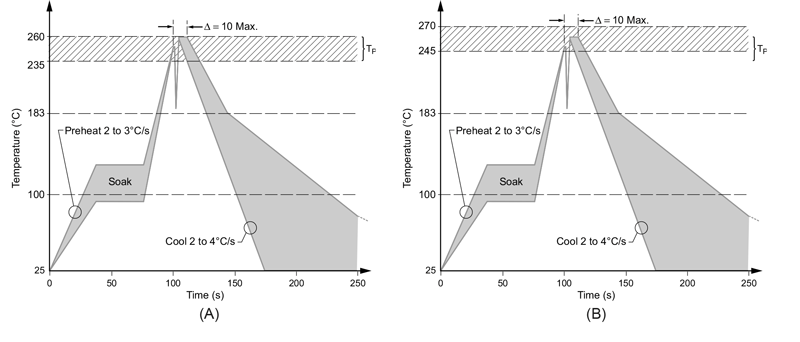
Figure 8 shows a typical higher temperature solder-reflow profile for SMD packages using traditional SnPb solder. Figure 9 provides a typical maximum solder-reflow profile for SMD packages, using Pb-free solders. Comparison of the two figures reveals the extent to which Pb-free processing may require higher maximum process temperatures.
Reflow soldering of through-hole devices is acceptable if the plastic body of the device is not exposed to excessive temperatures. Exceptions to the above are the SL package type, which has a thermoplastic housing that can deform if exposed to such high temperatures. If it is necessary to perform a reflow process on these packages, a special protective pallet must be built to shield the package so that the temperature of the housings does not exceed 210°C.
The following package types contain internal discrete soldered components and cannot be reflow soldered above 230°C max: KH, NB, PA, SM, SN, SP, SQ, UB, UC,
UD, UE, UF, and UG. Refer to the datasheets and MSL/ PSL labeling on the package box for details and contact Allegro Marketing.
Package types with exposed pads are difficult to solder on their total contact area; the general specs are >50%. The actual data for temperature rise with less contact (more solder voids) shows that 80% voids are safe for most applications and ambient operating temperatures.
Wave Soldering
Wave soldering of SMD packages is not generally recommended by Allegro but can be accommodated by customers with special attention of package to PCB adhesion and the use of as low a temperature as practical.
Allegro through-hole devices are designed to be used in a wave-soldering process. A typical wave-solder profile is shown in Figure 10.
When performing wave soldering, adequate spacing between the body of the device and the board should be maintained, and only halide-free fluxes should be used. For ACS75x current sensor package CA or CB, which have very high thermal mass, a preheat ramp rate of 2 to 5°C/s may be used.
Rework
Frequently, when a device that has been soldered on a PCB is removed, mechanical damage can occur to the device, such as internal delaminations. Before removing a device, a full qualified reflow profile should be completed, observing prebake and other MSL precautions, and no attempt to remove the device should be attempted before or after the solder has fully reflowed, and the device can be removed with minimal mechanical effort.
Rework with a Pb-free process may require an adjustment to procedures. For example, using a soldering iron and standard copper braid tape (with pre-embedded flux) to wick residual reflowed solder may require depositing a few drops of halide-free flux onto the tape to enable better flow.
Rework with a specialized point source hot air setup can run to very high temperatures, so it is important to limit the dwell time at temperature and remove the part from the PCB as soon as it reflows to avoid heat damage to the part.
Even when following appropriate procedures to remove a device, remounting of the device is typically not practical, and Allegro does not recommend reusing devices. The heating and exposure of terminals during mounting and removal oxidizes the terminal finishes, reducing the ability to wet. When remounting is attempted and fails, additional oxidization occurs, requiring remounting to take place at temperatures significantly above the original reflow profile at levels that may damage the device or the surrounding PCB components.
When reworking a device mounting, the following procedure is recommended:
- Carefully remove the previous device, using MSL precautions as described above.
- Thoroughly clean all solder and flux residues from the rework site.
- Stencil or pneumatically apply new solder paste on to the lands.
- Mount the new device.
- Prebake and reflow the site using qualified profiles.
- Complete the qualified reflow profile cooling cycle.
Joint Preservation
After removal of flux residue, the solder joint should be protected from moisture and potentially corrosive contaminants by applying a conformal coating to the assembled PCB. Allegro highly recommends this step, which has been demonstrated to be extremely effective, both in HAST (High Acceleration Stress Testing) and in fielded applications in harsh environments.
The preferred coating material is urethane. Alternatively, silicone can be used. The coating should be applied over the solder joints, terminals, and device case as a minimum. Other coatings such as epoxy, modified acrylics or paraleyne can also be used. For more reliability in coverage, the coating should be applied to the entire PCB assembly whenever practicable.
Circuit Design
The thermal conductivity of the application can affect the soldering results on an individual terminal basis. This is particularly noticeable with signal ground terminals that are connected to large ground planes, and with terminals that are connected to significant areas of exposed cop- per traces or connected by short traces to other nearby components.
These objects can all act as heat sinks, and additional heat soak time or a higher reflow temperature should be considered for such terminals.
Device packages with exposed thermal pads under the package body may require additional considerations. The PCB board has through-hole vias where the exposed pad will be placed. If there is a concern for thermal performance with the device because of power factors, one may want to minimize any voiding of the solder joint under the pack- age. Pre-solder filling of the PCB via holes may help to ensure that solder is not sucked down into the holes at the time of reflow leaving solder voids.
Solderability Testing
A common method of testing solderability is the “dip-and-look” method. However, for this method to yield accurate results, the terminals of the device under test must be preheated for a period of time that is adequate for their thermal characteristics. Devices with very long leads, for example through-hole devices such as the Allegro K pack- age, typically require an optimum heat soak of 5 seconds, as described in the J-STD-002 standard.
Additionally, wetting balance (meniscograph, for example) solderability testing can be done that is a more quanti- tative rather than qualitative solderability test. Allegro devices undergo such solderability tests at the end of package assembly operations and during qualifications to ensure compliance. Solderability with 100% tin plating or pre-plated terminations is acceptable even to 15 years storage life.
CONCLUSION
Through careful adherence to standard assembly procedures and MSL-based handling protocols, Allegro devices provide reliable performance. Contact an Allegro sales or service office for additional information on device handling and assembly.
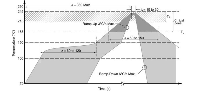
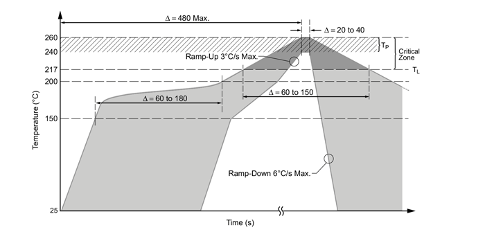
Figure 9. Solder Reflow Profile for SMD Using Lead (Pb) Free Solder. The typical acceptable maximum temperature range, TP, is 235°C to 260°C (shaded area), with 240°C to 250°C the preferred range. Temperatures refer to upper surface of the package case. Customers are responsible for determining their reflow profile suitable to their parts set, PCB, and reflow oven type; the above are only guidelines showing the range normally used. For 210°C or 230°C maximum package types, adjust profile accordingly.
Copyright 2020, Allegro MicroSystems.
The information contained in this document does not constitute any representation, warranty, assurance, guaranty, or inducement by Allegro to the customer with respect to the subject matter of this document. The information being provided does not guarantee that a process based on this information will be reliable, or that Allegro has explored all of the possible failure modes. It is the customer’s responsibility to do sufficient qualification testing of the final product to ensure that it is reliable and meets all design requirements.
Copies of this document are considered uncontrolled documents.