3D Linear or 2D Angle Sensing with the ALS31300 and ALS31313 Hall-Effect ICs
By Wade Bussing and Robert Bate,
Allegro MicroSystems, LLC
Abstract
This application note describes the use of the ALS31300 and ALS31313 3D Magnetic Linear Hall-Effect Sensor integrated circuits (ICs) from Allegro MicroSystems for 3D linear sensing and 2D angle sensing applications. References throughout this application note to the ALS31300 also apply for the ALS31313, except that the ALS31300 is provided in a 10-contact DFN package, and the ALS31313 is provided in a TSSOP-8 package.
Detailed examples include converting register contents to gauss for linear sensing, and combining data from two axes to calculate an angle for rotational angle sensing. Other sections describe the process of reading and writing registers on the ALS31300 via the I2C interface, application schematics, and the associated Arduino example code. See Appendix A for full source code, including an Arduino .ino sketch file. The Arduino .ino sketch file is also available on Allegro’s Software Portal.
Introduction
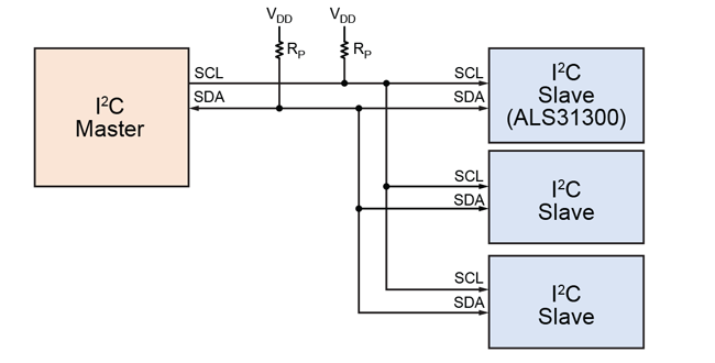
The ALS31300 3D Linear Hall-Effect Sensor IC provides users with an accurate, low-cost solution for non-contact linear and angular position sensing. With its I2C interface, the ALS31300 provides convenient access to angle and linear information from multiple sensors on a single bus (see Figure 1).
Examples listed in this application note make use of the “Teensy” 3.2 microcontroller (https://www.pjrc.com/teensy/teensy31.html) and Arduino (https://www.arduino.cc/) software environment. While this document focuses on implementation using the Teensy 3.2, the practices and example code translate directly to other Arduino boards.
I2C Overview
The I2C bus is a synchronous, two-wire serial communication protocol which provides a full-duplex interface between two or more devices. The bus specifies two logic signals:
- Serial Clock Line (SCL) output by the Master.
- Serial Data Line (SDA) output by either the Master or the Slave.
The block diagram shown below in Figure 1 illustrates the I2C bus topology.
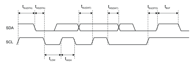
Data Transmission
The transmission of data over I2C is composed of several steps outlined in the sequence below.
- Start Condition: Defined by a negative edge of the SDA line, initiated by the Master, while SCL is high.
- Address Cycle: 7-bit Slave address, plus 1 bit to indicate write (0) or read (1), followed by an Acknowledge bit.
- Data Cycles: Reading or writing 8 bits of data, followed by an Acknowledge bit. This cycle can be repeated for multiple bytes of data transfer. The first data byte on a write could be the register address. See the following sections for further information.
- Stop Condition: Defined by a positive edge on the SDA line, while SCL is high.
Except to indicate Start or Stop conditions, SDA must remain stable while the clock signal is high. SDA may only change states while SCL is low. It is acceptable for a Start or Stop condition to occur at any time during the data transfer. The ALS31300 will always respond to a Read or Write request by resetting the data transfer sequence.
The clock signal SCL is generated by the Master, while the SDA line functions as either an input or open-drain output, depending on the direction of data transfer. Timing of the I2C bus is summarized in the timing diagram in Figure 2. Signal references and definitions of these names can be found in the ALS31300 datasheet.
I2C Bus Speeds
Common I2C bus speeds are 100 kbps standard mode and the 10 kbps low-speed mode, but arbitrarily low clock frequencies are also allowed. Recent revisions of the I2C protocol can host
more nodes and run at faster speeds including 400 kbps fast mode and 1 Mbps fast mode plus (Fm+) which are all supported by the ALS31300. Note the spec outlines an additional 3.4 Mbps highspeed mode that is not supported by ALS31300.
Implementation of I2C with the ALS31300
The ALS31300 may only operate as a Slave I2C device, therefore it cannot initiate any transactions on the I2C bus.
The ALS31300 will always respond to a Read or Write request by resetting the data transfer sequence. The state of the Read/Write bit is set low (0) to indicate a Write cycle and set high (1) to indicate a Read cycle. The Master monitors for an Acknowledge bit to confirm the Slave device (ALS31300) is responding to the address byte sent by the Master. When the ALS31300 decodes the 7-bit Slave address as valid, it responds by pulling SDA low during the ninth clock cycle. When a data write is requested by the Master, the ALS31300 pulls SDA low during the clock cycle, following the data byte to indicate that the data has been successfully received. After sending either an address byte or a data byte, the Master must release the SDA line before the ninth clock cycle, allowing the handshake process to occur.
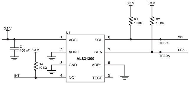
The default slave address for the ALS31300 is 110xxxx, where the four LSB bits are set by applying different voltages to the address pins ADR0 and ADR1. Both address pins have been set to ground for this demonstration as shown by the schematic in Figure 11. For information on selecting other I2C Slave addresses, refer to the ALS31300 datasheet. With both pins grounded, the default I2C Slave address is 96.
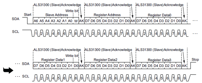
Write Cycle Overview
The write cycle to access registers on the ALS31300 are outlined in the sequence below.
- Master initiates Start Condition
- Master sends 7-bit slave address and the write bit (0)
- Master waits for ACK from ALS31300
- Master sends 8-bit register address
- Master waits for ACK from ALS31300
- Master sends 31:24 bits of data
- Master waits for ACK from ALS31300
- Master sends 23:16 bits of data
- Master waits for ACK from ALS31300
- Master sends 15:8 bits of data
- Master waits for ACK from ALS31300
- Master sends 7:0 bits of data
- Master waits for ACK from ALS31300
- Master initiates Stop Condition
The I2C write sequence is further illustrated in the timing diagrams below in Figure 3.
Customer Write Access
An access code must be sent to the device prior to writing any of the volatile registers or EEPROM in the ALS31300. If customer access mode is not enabled, then no writes to the device are allowed. The only exception to this rule is the SLEEP bit, which can be written regardless of the access mode. Furthermore, any register or EEPROM location can be read at any time regardless of the access mode.
To enter customer access mode, an access command must be sent via the I2C interface. The command consists of a serial write operation with the address and data values shown in Table 1. There is no time limit for when the code may be entered. Once the customer access mode is entered, it is not possible to change access modes without powercycling the device.
Table 1: Customer Access Code
| Access Mode | Address | Data |
| Customer Access | 0x35 | 0x2C413534 |
Read Cycle Overview
The read cycle to access registers on ALS31300 is outlined in the sequence below.
- Master initiates Start Condition
- Master sends 7-bit slave address and the write bit (0)
- Master waits for ACK from ALS31300
- Master sends 8-bit register address
- Master waits for ACK from ALS31300
- nitiate a Start Condition. This time it is referred to as a Restart Condition
- Master sends 7-bit slave address and the read bit (1)
- Master waits for ACK from ALS31300
- Master receives 31:24 bits of data
- Master sends ACK to ALS31300
- Master receives 23:16 bits of data
- Master sends ACK to ALS31300
- Master receives 15:8 bits of data
- Master sends ACK to ALS31300
- Master receives 7:0 bits of data
- Master sends NACK to ALS31300
- Master initiates Stop Condition
The I2C read sequence is further illustrated in the timing diagrams below in Figure 4.
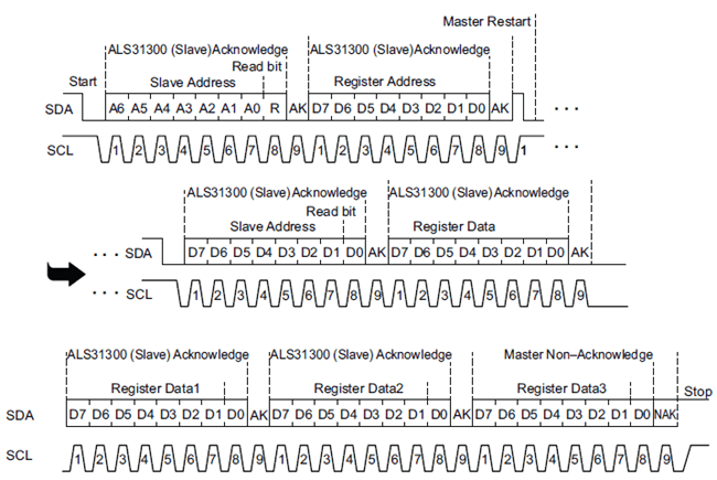
The timing diagram in Figure 4 shows the entire contents (bits 31:0) of a single register location being transmitted. Optionally, the I2C Master may choose to replace the NACK with an ACK instead, which allows the read sequence to continue. This case will result in the transfer of contents (bits 31:24) from the following register, address + 1. The master can then continue acknowledging, or issue the not-acknowledge (NACK) or stop after any byte to stop receiving data.
Note that only the initial register address is required for reads, allowing for faster data retrieval. However, this restricts data retrieval to sequential registers when using a single read command. When the Master provides a not-acknowledge bit and stop bit, the ALS31300 stops sending data. If non-sequential registers are to be read, separate read commands must be sent.
I2C Readback Modes for X, Y, Z and Temperature Data
The ALS31300 I2C controller has several modes to make the process of repeatedly polling X, Y, Z and Temperature data convenient. These options include Single Mode, Fast Loop Mode and Full Loop Mode.
Single Mode
A single write or read command to any register—this is the default mode and is best suited for setting fields and reading static registers. If desired, this mode can be used to read X, Y, Z and Temperature data in a typical serial fashion, but fast or full loop read modes are recommended for high-speed data retrieval.
Fast Loop Mode
Fast Loop Mode offers continuous reading of X, Y, Z and temperature values, but is limited to the upper 8 bits of X, Y, Z and upper 6 bits of Temperature. This mode is intended to be a time-efficient way of reading data from the IC at the expense of truncating resolution. The flow chart in Figure 5 depicts Fast Loop Mode.
Full Loop Mode
Full Loop Mode provides continuous reads of X, Y, Z and Temperature data with full, 12 bit resolution. This is the recommended mode for users wanting a higher data rate for X, Y, Z and Temperature with full resolution. The flow chart in Figure 6 depicts Full Loop Mode.

The Looping modes are further described below in Table 2.
Table 2: ALS31300 Looping Read Modes
| Code (Binary) | Mode | Description |
| 00 | Single | No Looping. Similar to Default I2C. |
| 01 | Fast Loop | X, Y, Z and Temperature fields are looped. 8 MSBs for X, Y, and Z; 6 MSBs for Temperature are looped. |
| 10 | Full Loop | X, Y, Z and Temperature fields are looped. Full, 12-bit resolution fields are looped. |
| 11 | Single | Same as code 0. |
To set the read loop mode, set bits 3:2 at address 0x27 to the desired code value per Table 2.
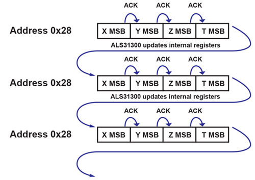
Magnetic Field Strength Registers
and ALS31313 TSSOP Package (right) (not to scale)
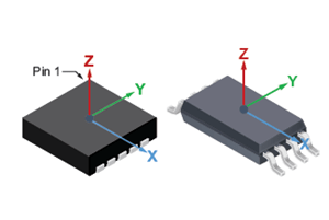
The magnetic field strength registers contain data that is proportional to the measured magnetic field in each of the three axes as seen by the ALS31300. The register addresses and bit fields for X, Y, and Z magnetic data are described in Table 3. The orientations of X, Y and Z Axes are defined in Figure 7.
The MSBs and LSBs of each axis must be concatenated to resolve full 12-bit magnetic field data. Refer to Appendix A for example code of various techniques to poll and concatenate the magnetic data from ALS31300.
Table 3: Magnetic Field Strength Registers
| Address | Bits | Name | Description | R/W |
| 0x28 | 31:24 | X Axis MSBs | 8 bit signal proportional to upper 8 bits of field strength in X direction. | R |
| 23:16 | Y Axis MSBs | 8 bit signal proportional to upper 8 bits of field strength in Y direction. | R | |
| 15:8 | Z Axis MSBs | 8 bit signal proportional to upper 8 bits of field strength in Z direction. | R | |
| 0x29 | 19:16 | X Axis LSBs | 4 bit signal proportional to lower 4 bits of field strength in X direction. | R |
| 15:12 | Y Axis LSBs | 4 bit signal proportional to lower 4 bits of field strength in Y direction. | R | |
| 11:8 | Z Axis LSBs | 4 bit signal proportional to lower 4 bits of field strength in Z direction. | R |
Temperature Sensor Registers
Temperature Registers of ALS31300 are described below in Table 5.
Table 4: Temperature Registers
| Address | Bits | Name | Description | R/W |
| 0x28 | 5:0 | Temperature MSBs |
6 bit signal proportional to upper 6 bits of temperature. |
R |
| 0x29 | 5:0 | Temperature LSBs |
6 bit signal proportional to lower 6 bits of temperature. |
R |
Calculating Measured Field
For this example the full-scale range of ALS31300 is 500 gauss, giving a sensitivity of 4 LSB/gauss.
The process begins with a full 8 byte read of MSB and LSB registers to construct a 12 bit, 2’s complement signed value. All data must be read in a single 8 byte read when combining registers, or the result will be the combination of two separate samples in time. The 12 bits of data are combined per Table 5.
Table 5: MSB and LSB Combination Data
| BIT | 11 | 10 | 9 | 8 | 7 | 6 | 5 | 4 | 3 | 2 | 1 | 0 |
| DATA | MSB Data | LSB Data | ||||||||||
Assume a full 8 byte read returns the following binary data for a single axis:
MSB = 1100_0000
LSB = 0110.
The combined data {MSB; LSB} = 1100_0000_0110. The decimal equivalent = –1018, which can be converted to gauss by dividing by the device sensitivity (4 LSB/gauss).
gauss = –1018 LSB ÷ 4 LSB⁄G = –254 gauss
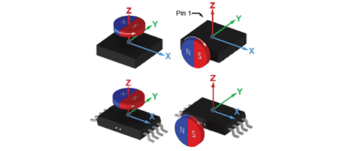
Calculating Angle Using Two Axes
The angle of an applied field can be calculated using magnetic data from two axes of the ALS31300 and a four quadrant arc tangent function. For this example, a disc magnet is magnetized diametrically. The drawings in Figure 8 show reference orientations of puck magnets and their poles compared to the X, Y, and Z axes of the ALS31300. In the left orientation, the magnet is rotating around the Z axis, as indicated by the white arrow, while sensing magnetics with X and Y. In the orientation on the right, the magnet is rotated about the Y axis, while using X and Z channels to sense. The third orientation can be used with a magnet rotating around the X axis and sensing with Y and Z.
Standard inverse tangent functions, i.e. tan()-1, return angle values ranging from –90° to 90°. For this application, it is important to use a four quadrant arc tangent function to return an angle from –180° to 180°. This function also avoids issues with dividing by 0. Four quadrant inverse tangent functions are listed in Table 6.
Table 6: Four Quadrant Arc Tan Function Calls
| Program | Function | Description |
| MATLAB | atan2(Y,X) | 4 quadrant tan-1. Result in radians. |
| atan2d(Y,X) | 4 quadrant tan-1. Result in degrees. | |
| ARDUINO | atan2(Y,X) | 4 quadrant tan-1. Returns double. |
| atan2f(Y,X) | 4 quadrant tan-1. Returns float. | |
| C# | Atan2(Y,X) | 4 quadrant tan-1. Returns double. |
Refer to Appendix A for full Arduino source code on calculating angle for XY, XZ, and YZ axes combinations.
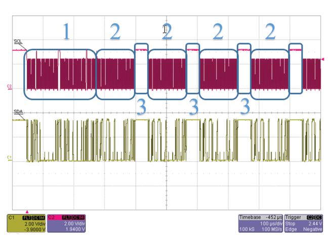
The conversion process can be summarized into 3 major steps, which are listed below and identified on the scope plot in Figure 9. “Single” mode (Table 2) is used to simplify this example.
- Read request is initiated by the Master.
- Transmission of 8 bytes of data from the Slave.
- Conversion of magnetic vector data to an angle value.
The read request (box 1) consists of a write to the device indicating which registers will be read. The device responds (box 2) with 8 bytes of data, (8 MSB of X, Y, Z and 6 MSB of temperature, followed by 4 LSB of X, Y, Z and 6 MSB of temperature).
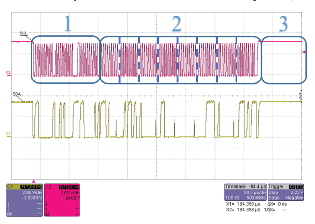
Registers 0x28 and 0x29.
Angle Calculation Timing
The total time to complete an angle calculation using the ALS31300 will be application specific, but predominantly dominated by the processing abilities and speed of the user’s microcontroller. Other factors include the loop mode of the ALS31300 (Table 2) and communication frequency of the I2C interface. Timing examples in this document assume a Teensy 3.2 microcontroller running at 72 MHz and configured I2C communication speed of 1 MHz (Fast Mode+). Note that the Teensy 3.2 Fast Mode+ I2C mode operates around 720 kHz.
The example in Figure 9 is a simple way to read data from the ALS31300, but it is not the fastest. The overhead of initiating a read (Box 1 in Figure 9) can be eliminated after the first request
through the use of loop modes on the ALS31300.
The scope plot in Figure 10 shows the angle conversion flow with ALS31300 set in Full Loop Mode. The boxes 1, 2, and 3 still correspond to the same steps from Figure 9.
Registers 0x28 and 0x29.
Notice that box 1 occurs only once, but is slightly longer than the No Loop example in Figure 9. In Full Loop Mode, the read request consists of a write to the device indicating which register will be read, followed by a read/write to set full loop mode. Refer to full source code in Appendix A on how to implement no loop, fast loop and full loop read modes.
The repeated pause in box 3 shows the time it takes Teensy 3.2 microcontroller to perform the atan2f(x,y) function. The average duration of the atan2f(x,y) function on the Teensy 3.2 at 72 MHz is 30 μs, while the transmit time of 8 data bytes is 120 μs. Using the Teensy 3.2 and ALS31300 in Full Loop Mode, a fresh angle value can be calculated every 150 μs.
Application Schematics
Refer to the image in Figure 11 showing the application schematic used for the ALS31300 throughout this document.
Supporting circuitry for the Teensy 3.2 microcontroller is shown in the schematic in Figure 12.
Refer to the nets labeled “SDA” and “SCL” in Figure 11 and Figure 12 indicating these connections between the two schematics. Note, the pin locations of SDA and SCL on the Teensy micro are user-selectable, but must be declared in software. Refer to the source code in Appendix A where the SDA and SCL pins are declared.
Conclusion
The ALS31300 is a highly versatile, micropower 3D Hall-effect sensor IC. The IC can be used for multi-axis linear position, or angular position sensing applications, and can be configured for operation in high resolution (12 bit) or medium resolution (8 bit) mode. The I2C bus is highly configurable, and can operate at bus speeds from 1 Mbps down to < 10 kbps, with a pullup voltage range of 1.8 to 3.3 V. The IC also includes a temperature sensor that can read over the I2C interface.
The Arduino .ino sketch file used with this application note is available on Allegro’s Software Portal. Register for the “ALS31300” device to view the source code.
The ALS31300 datasheet is available at https://www.allegromicro.com/en/Products/Magnetic-Linear-And-Angular-Position-Sensor-ICs/Linear-Position-Sensor-ICs/ALS31300.aspx.
The ALS31313 datasheet is available at https://www.allegromicro.com/en/Products/Magnetic-Linear-And-Angular-Position-Sensor-ICs/Linear-Position-Sensor-ICs/ALS31313.aspx.
APPENDIX A: Full Arduino Source Code for ALS31300 and Teensy 3.2
The snippet below shows full Arduino source code used alongside this application. Example functions include I2C initialization, reading from the ALS31300 in single, fast, and full loop modes, writing data to the ALS31300 using I2C and calculating angle and gauss using magnetic data from the ALS31300.
The full .ino Arduino sketch is available on Allegro Microsystem’s Software portal under the ALS31300 device tab. To register with Allegro’s software portal and view the ALS31300 source code, visit https://registration.allegromicro.com/login.
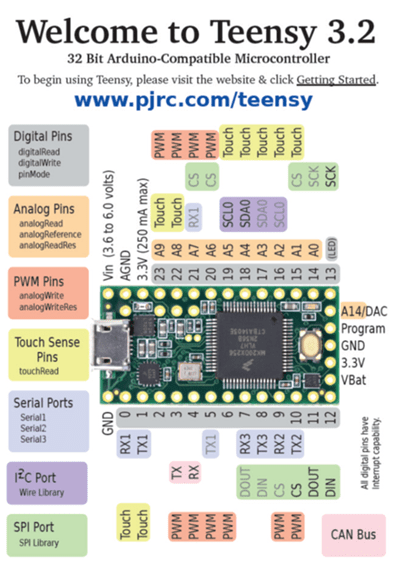
APPENDIX B: TEENSY PINOUT FLYER
The pinout flyer below ships with each Teensy 3.2. It is also available from PJRS at the following link: https://www.pjrc.com/teensy/card7a_rev1.pdf.
The information contained in this document does not constitute any representation, warranty, assurance, guaranty, or inducement by Allegro to the customer with respect to the subject matter of this document. The information being provided does not guarantee that a process based on this information will be reliable, or that Allegro has explored all of the possible failure modes. It is the customer’s responsibility to do sufficient qualification testing of the final product to insure that it is reliable and meets all design requirements.