Non-Intrusive Hall-Effect Current-Sensing Techniques Provide Safe, Reliable Detection and Protection for Power Electronics
By Paul Emerald
Abstract
As systems extend and expand the exploitation of the latest power semiconductors (IGBTs, MCTs, etc.) that manifest the very relentless advance in power output limits, a prerequisite (and parallel) demand for sensing these escalating current levels is (increasingly) very apparent. Hall-effect ICs provide 'non-intrusive' current sensing techniques and safe, isolated detection of high current levels without dissipating the sizable amounts of wasted power (and the resultant heating) associated with resistive current-sensing methods. Further, Hall-effect current sensing provides electrical isolation of the current-carrying conductor; hence, a safe environment for circuitry, operators, etc.
The proliferating current-sensing applications for Hall-effect sensor ICs continue; become even more diverse; plus expand and grow as other designers endeavor to protect systems, create more reliable 'bulletproof' equipment, and reconcile any safety issues. The prime applications for cost-effective Hall-effect sensor ICs for current sensing include:
- Current Imbalance
- Current Monitoring
- Operator/User Safety and Security
- Overcurrent Detection/System Protection
- System Diagnosis and Fault Detection
- Test and Measurement
Background and Introduction
The discovery of the Hall-effect originated back in 1879; however, any meaningful application of this Edwin H. Hall finding awaited semiconductor integration that first occurred in the late 1960s. Subsequently, further advances (particularly those of the 1990s) have evolved further, more fully functional integration plus an expanding series of application-specific Hall sensor IC types. Yet the relentless progress of magnetic sensor electronics continues to proliferate an increasing demand for low-cost, reliable, and 'non-contact' Hall-effect circuitry for sensing/detecting motion, direction, position, and measuring/monitoring current.
Hall-effect sensor ICs (especially the ratiometric linear types) are superb devices for 'open-loop' current-sensing designs. However, there are limits to the operational range, accuracy and precision, frequency response, etc. that may be realized. Because many prospective users are ignorant of and/or oblivious to either the benefits or shortcomings of current-sensing techniques using Hall-effect ICs, this paper endeavors to provide a comprehensive discussion of the essential, basic techniques of 'non-intrusive' current sensing with silicon Hall-effect devices (HEDs) now available.
Most Hall-effect current-sensing requirements do not develop adequate magnetic fields without the use of a slotted toroid to concentrate (and focus) the induced flux field. Low-to-modest currents (<≈ 15 amperes) require winding sufficient turns on the slotted toroid (core) to induce usable flux strength and develop a suitable signal voltage. A higher current level (>15 to 20 amperes) induces field intensities that allow passing the current-carrying conductor straight through the center of the toroid (no turns necessary at these higher currents).
Designs requiring a broad (or continuous) current range mandate utilizing linear Hall-effect sensor ICs. However, overcurrent protection and/or fault detection designs can be accommodated by digital HEDs. Examples and particulars of the essentials of current-sensing techniques, device parameters, temperature stability, and other relevant concerns of Hall-effect current sensing are covered in this treatise on HEDs for sensing AC and DC currents.
Rival, Competing Technologies
Although there are many current-sensing methods, only three are commonplace in low-cost, volume applications. The others are expensive laboratory systems, emerging technologies (magnetoresistive is an example), or seldom used. The commonly used techniques include: (1) resistive, (2) Hall effect, and (3) current transformers.
Resistive sensing is very widely used, low-cost, and understood with little difficulty. However, the shortcomings are its insertion loss (heating and wasted power) and lack of isolation. Also, the series inductance of many power resistors constrains the frequency range with low-cost components; hence, resistive sensing is classed as either a DC or AC application per the categories in table 1. Low inductance, high-power resistors for high frequency are more expensive, but allow operation beyond 500 kHz. Further, signal amplification is (usually) required with resistive current-sensing techniques (either a comparator or operational amplifier is needed).
| Table 1: Commonplace, Inexpensive Current-Sensing Techniques | |||||||
|---|---|---|---|---|---|---|---|
| Widely Used Sensors | Power Consumption |
Circuit Isolation | Frequency Range | Size | Accuracy | Relative Cost | |
| Insertion Loss | External Power | ||||||
| Sense Resistor + Op-Amp | High | Low | Low | DC to 10 MHz | Medium | ±3 to 5% | Low |
| Standard Open Loop Hall-Effect | Low | Low | High | DC to 50 kHz | Small | ±5 to 10% | Medium |
| Hall-Effect Closed-Loop | Low | Medium | High | DC to 1 MHz | Medium to Large | < ±1% | High |
| Allegro Open-Loop Hall Effect Current Sensor ICs | Low | Low | High | DC to 120 kHz | Small | ±2 to 3% | Medium |
| Current Transformers | Medium (AC) | None | high | 60 Hz to 1 MHz* | Medium to Large | ±3 to 5% | High |
| * Current transformers usually operate over a limited frequency range but can be designed for use from low to high frequencies. | |||||||
Hall-effect sensor ICs (open- and closed-loop) represent the next tier of commonplace solutions. Insertion loss (and related heating, etc.) are not an obstacle. However, frequency range, cost, DC offset, and external power represent the potential disadvantages of Hall-effect IC technology when compared to the resistive-sensing methods.
Current transformers close out the last low-cost technology, and (as the term transformer should imply) are only useful with alternating currents. Most low-cost current transformers are designed for narrow frequency ranges, are more expensive than resistive or Hall-effect, and cannot be used for DC currents. However, current transformers avoid insertion loss, offer electrical isolation, do not require external power, and exhibit no offset voltage at the zero (null) current level.
Because this treatise focuses upon Hall-effect ICs, understanding the elements of linear, ratiometric HEDs is imperative to open-loop current sensing.
Linear Hall-Effect Sensor ICs
As the term implies, linear Hall sensor ICs develop an output signal that is proportional to the applied magnetic field. Normally, in any current-sensing application, this flux field is focused by a 'slotted' toroid to develop an adequate field intensity, and this magnetic field is induced by current flowing in a conductor. A 'classic' transfer curve for a ratiometric linear is illustrated in figure 1. Note that, at each extreme of its range, the output saturates.
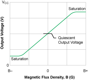
Figure 1. Linear Hall Sensor IC Transfer Curve
Most recent linear Hall ICs provide a ratiometric output voltage. The quiescent (i.e., null) voltage is (nominally) 50% of the applied, stable supply. This quiescent output voltage signal equates to no applied magnetic field and, for current sensing, is equivalent to zero current flow. A south polarity field induces a positive voltage transition (toward VCC), and a north polarity results in a transition toward ground (0 V). Output saturation voltages are (typically) 0.3 V (high/sourcing) and 0.2 V (low/ sinking) and are measured at ±1 mA. [Ed. Note. output voltages are now in the multivolt range.]
Each linear Hall-effect IC integrates a sensitive Hall element (also called a 'plate'), a low-noise (bipolar) amplifier, and sink/ source output stage. Any systems problems associated with low-level signals and noise are minimized by the monolithic integration of magnetic Hall element, amplifier, output, and allied signal processing circuitry.
Existing very stable, linear HEDs exploit dynamic quadrature offset cancellation circuitry and utilize electronic switching to change the current path in the Hall element. Switching the current paths, from 0° to 90°, at a high repetition rate offers a new answer to the (intrinsic) DC offset that has long plagued linear sensor IC operation and stability.
Sample-and-hold circuitry and a low-pass filter are exploited to properly 'recondition' the internal dynamic signals of these innovative linear HEDs.
Linear Hall-effect ICs can detect small changes in flux intensity, and are (generally) more useful than digital Hall ICs for current sensing. Linear HEDs are often capacitively coupled to op amps, or DC connected to comparators, to attain system design objectives. Also, microcontrollers (µCs) and microprocessors (µPs) are being exploited to detect small signal changes from linear Hall ICs, and are very suitable (with proper software) for sensing/measuring either AC or DC currents.
Inducing a Magnetic Field
As mentioned, Hall-effect current sensing usually necessitates the use of a slotted toroid (made of ferrous materials). The toroid both concentrates and focuses an induced magnetic field toward the location of the Hall-effect element within the IC package. Figure 2 typifies a classic example of 'non-intrusive' current sensing exploiting a slotted toroid. The conductor current flows through the turns wound upon the toroid, and the induced flux field is concentrated on the sensor IC in the gap (or slot) in the toroid. Usually, this gap is made to closely match the Hall IC package thickness ( approx. 0.060" or 1.52 mm), and this provides optimal magnetic coupling. The current flow (with this 'tight' magnetic coupling) induces a flux intensity per the formula
B (gauss) ≈ N (turns) × 6.9 gauss/ampere
[Ed. Note: 6.9 gauss/ampere is updated from the earlier 6 gauss/ampere.]
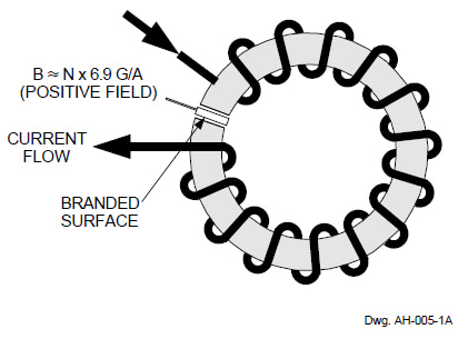
Figure 2. Current Sensing with Gapped Toroid
Widening the slot (gap) reduces the flux coupling and can increase the upper current limit, which is predicated upon the Hall sensor IC sensitivity (more to follow). However, decoupling the induced field to extend the maximum current limit may affect linearity, usable range, etc. This 'loose' coupling is under evaluation, but not yet complete; hence, no new formulas for magnetic flux and conductor current (and larger gaps) have been documented.
'Calibrated' Ratiometric Linear HEDs
The two newest [Ed. Note: Article originally presented in 1997.] linear Hall sensors, with dynamic DC offset cancellation, provide a cornerstone for a discourse on linear ratiometric HEDs and current sensing. The A3515 plot (figure 3) and related data (table 2) record the vital characteristics of the most sensitive linear HED; its counterpart, the A3516, properties are in figure 4 and table 3.
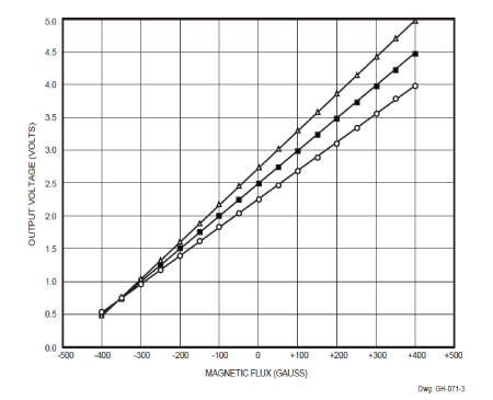
Figure 3. Linear, Ratiometric Hall-Effect Device Characteristics (A3515 Output)
| Table 2: Linear, Ratiometric Hall-Effect Device Characteristics Measurement Data (A3515), Measured Over ±250 Gauss |
|||||
|---|---|---|---|---|---|
| Marker | VCC (Volts) |
VOQ (Volts) |
Sensitivity (mV/G) |
Non-Linearity (%) |
Symmetry (%) |
| Circle | 4.500 | 2.217 | 4.450 | ≤0.1 | 99.9 |
| Square | 5.000 | 2.463 | 5.014 | ≤0.2 | 99.9 |
| Triangle | 5.500 | 2.710 | 5.704 | ≤0.1 | 99.7 |
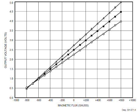
| Table 3: Linear, Ratiometric Hall-Effect Device Characteristics Measurement Data (A3516), Measured Over ±500 Gauss |
|||||
|---|---|---|---|---|---|
| Marker | VCC (Volts) |
VOQ (Volts) |
Sensitivity (mV/G) |
Non-Linearity (%) |
Symmetry (%) |
| Circle | 4.500 | 2.232 | 2.149 | ≤0.1 | 99.9 |
| Square | 5.000 | 2.475 | 2.481 | ≤0.1 | 99.6 |
| Triangle | 5.500 | 2.723 | 2.820 | ≤0.1 | 99.9 |
Presently, though seldom sold, 'calibrated' linear Hall-effect ICs are superb circuits for setting up and measuring system magnetic parameters, and represent an excellent entry to the performance, characteristics, and limitations of ratiometric ICs.
Sensor Sensitivity
The elemental distinction between the A3515 and A3516 is magnetic sensitivity. The nominal data for the two specific sensor ICs depicted in figures 3 and 4 is listed in tables 2 and 3. Sensitivity is specified in millivolts per gauss (mV/G). Three voltages are listed; however, most designs utilize fixed, low-cost 5 V regulator ICs for stability. The nominal sensitivity (and usable range) of the two linear HEDs is as follows (VCC = 5 V):
- A3515
- Sensitivity: 5.0 mV/G
- Range: ≥±400 G (≥±2.0 V)
- A3516
- Sensitivity: 2.5 mV/G
- Range: ≥±800 G (≥±2.0 V)
Linearity and Symmetry
From these plots (figures 3 and 4) it is apparent that neither linearity nor symmetry (the deviation in the slope from the quiescent (or null) voltage) is a vital design consequence as neither surpasses 0.3% for the A3515. The plots record ±400 G for the A3515, and ±800 G for the A3516, and output voltage swings of ≥±2.0 V for both types.
Linear Current Range(s)
The practical current limit (maximum with 'tight' coupling) is derived using the range and flux per turn in the prior formula per the approximation:
- A3515: ≥±400 G ÷6.9 G/A ≈ ±58 A
- A3516: ≥±800 G ÷6.9 G/A ≈ ±116 A
Per a prior mention, current values beyond ≈ 115 amperes mandate reducing the magnetic coupling, shunting higher current levels (i.e., pass a portion of the total through the toroid), or other methods that effectively 'desensitize' the circuitry. There are many, growing and expanding applications for 'non-intrusive' current sensing, especially at high currents (>100 A).An ultra-low value resistor (<1 mΩ) dissipates considerable power and heating at these currents, and the 'non-inductive' resistors needed raise costs. I2R losses cannot be avoided; a sense resistor of 500 mΩ and 200 A produces 20 watts. Obviously, this is a situation that a designer would prefer to avoid. However, low-cost options are scarce (or non-existent). [Ed. Note: The Allegro™ ACS75x current sensor IC series is now available, which can accommodate currents up to the ±200 A range.]
Linear, Ratiometric Hall-Effect ICs
The latest linear HEDs incorporating the dynamic quadrature DC offset cancellation are illustrated in figure 5. The Hall element is a 'single-plate,' and designated by its symbol (Χ). Sensor IC current is switched from a 0° orientation (downward) to a 90° path (across the Hall plate) at ≈ 170 kHz. This precludes most of the earlier offset related factors (DC imbalances due to resistive gradients, geometrical dissimilarities, piezoresistive effects, etc.). A low-pass filter and a sample-and-hold circuit are employed to recondition the signal fed to the linear, ratiometric Hall sensor IC output.
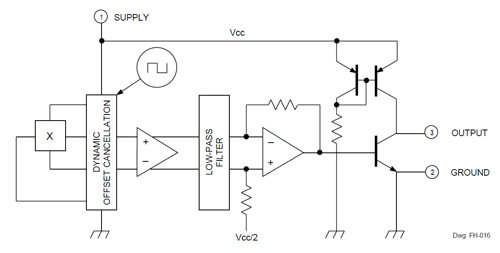
Figure 5. Linear Hall-Effect Sensor with Dynamic Quadrature Offset Cancellation
Powering Linear Hall-Effect ICs
Although the power requirements for linear HEDs are small, external power is needed. The source must be stable and well regulated; and with fixed voltage IC regulators (usually 5 V) this design issue is simply (and inexpensively) resolved. The linear sensor ICs specify a maximum supply current of ≤10 mA with 5 V (typical value ≈ 7 mA). Easy, on-board, 'down' regulation from a system supply is simple with low-cost IC regulators.
A listing of absolute maximum limits for the new linear, ratiometric sensor ICs follows in table 4.
| Table 4: Absolute Maximum Limits (TA= 25°) |
|
|---|---|
| Characteristic | Rating |
| Supply Voltage, VCC | 8.0 V |
| Output Voltage, VOUT | 8.0 V |
| Output Sink Current, IOUT | 10 mA |
| Magnetic Flux Density, B | Unlimited |
| Package Power Dissipation, PD | 600 mW* |
| * 'UA' package rating of 183°C/W. [Ed. Note: Rating is 184.] | |
Operation beyond the above specified limits may affect device operation, performance, or result in compromising (sacrificing) circuit and/or system reliability and is (absolutely) not recommended.
Maximum Supply Voltage − The recent linear HEDs, with offset cancellation, permit operation at a higher supply than the prior generation (A3506, etc.). These new linear ICs boost the maximum limit to that of table 4.
Maximum Output Voltage − Also itemized in table 4; however, it should be noted that the output must not be connected to a voltage either beyond the supply or below the IC ground. Either might compromise the Hall sensor IC reliability and/or affect system dependability.
Maximum Output Current − The newest linear HEDs specify a higher current than prior devices. However, typical applications rarely involve more than a trivial percentage of the 10 mA maximum listed in table 4. The high-impedance inputs of today's analog or conversion circuitry (usually) necessitates microamperes not milliamperes of Hall sensor IC output current.
Maximum Flux Density − Magnetic fields that exceed the linear range of these Hall-effect ICs neither damage nor destroy the device. However, magnetic fields beyond the usable range force the output into saturation (and non-linear operation) without harm to the HED.
Package Power Dissipation−The maximum package power dissipation limit is based upon operating with safe, reliable junction temperatures. The two package types in use are specified below for their thermal resistance (and maximum power with TA = +25°C).
- 'U' Package: RθJA = 183°C/W (P D = 683 mW)
[Ed. Note: RθJA rating of 184 is correct.] - 'UA' Package: RθJA = 206°C/W (P D = 606 mW)
[Ed. Note: RθJA rating of 165 is correct.]
The maximum recommended junction temperature is 150° [Ed. Note: Now up to 165°C.] and the dissipation should equal zero at this temperature. However, the newest linears permit infrequent (i.e., transient) excursions up to 200°C (ambient temperature, TA ≤ 170°C).
The internal power (PD) consists of two factors: (a) the HED supply power (ICC × VCC) and (b) the IC output power (IOUT × VOUT(SAT) ). Normally, supply power (a) smothers output dissipation (b), and for 5 V operation typical power dissipation is ≤40 mW. With ≤40 mW, the device junction temperature might rise ≈ 8°C above the ambient (TJ ≤ TA + [PD × RθJA]).
Internal power is (usually) not a HED limitation, but designers should comprehend the basic results of device power dissipation and its relationship to elevating the sensor IC junction temperature. IC (and system) reliability is inversely correlated to the temperature of all system components. Higher ambient and junction temperatures reduce the life expectancy and dependability of any system.
Distinctive Linear HED Parameters
Various, numerous linear-HED characteristics are of concern in current-sensing applications, and brief descriptions of these follow. Subsequently, many of these characteristics and parameters will be embodied in a focus on accuracy, temperature effects, linearity, symmetry, etc.
Voltage Output − As mentioned, the ratiometric, linear Hall sensor ICs provide an output voltage that is proportional to the applied magnetic field induced by current as illustrated in figure 2. The output is specified to sink and source ±1 mA at guaranteed limits. Per figures 2, 3, and 4, the usable range is ≥±2.0 V with a 5 V supply. Also previously mentioned, the quiescent output voltage is 1 ⁄ 2 the supply when no magnetic field is present (or current induced). A stable, well-regulated supply is very necessary for proper operation, otherwise the output voltage will fluctuate and follow any variations in supply. [Ed. Note: For latest performance characteristics, refer to the Allegro selection guide.]
Circuit Loading with Hall-Effect Sensor ICs − The linear HEDs present no load to the conductor being sensed. A 'no-disconnect,' 'non-intrusive' technique is based upon forming a 'toroid' around the conductor being sensed. Rather than pass the wire through the toroid (figures 6A and 6B), a soft iron piece is formed around the conducting wire. This permits sensing currents without the need for disconnecting any conductors in the power system ('no-disconnect' formed toroid is shown in figure 6C).
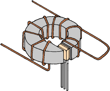
Figure 6A. Toroidal Current Sensing Application(<15 A)
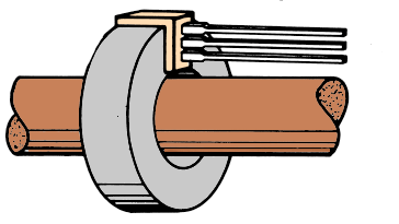
Figure 6B. Toroidal Current Sensing Application(>15 A)
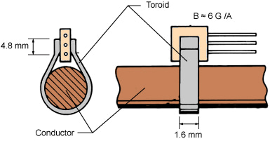
Figure 6C. 'No-Disconnect' Current Sensing Application
Tolerance to Current Overloads − As mentioned, a conductor current that exceeds the range of the linear Hall IC forces the output into a non-linear, saturated condition. Excessive current does not impair or damage the sensor IC. However, extreme, sustained overcurrent could be a fire or safety hazard if the conductor overheats and creates a dangerous situation.
Response Time of Hall-Effect Current Sensors − A review of some of the current sensing devices utilizing Hall-effect-based techniques and toroids reveals a rather broad range of sensor IC response times. A majority of these (those including amplifiers) fall within a range of ≈ 7 ms to ≈ 15 ms, though others are below and above these limits. Testing is (normally) specified with di/dt = 100 A/ms; and the specified linear current ranges vary from rather low (<5 A) to the extreme (>20,000 A). Obviously, the 20 kA variety are expensive and do not exploit any low-cost toroid techniques.
Hall-Effect Sensor IC Bandwidth − Today, the usable bandwidth of most linear Hall ICs is ≥ 20 kHz. Signal voltage changes little up to this frequency. However, noticeable phase shift becomes distinct at somewhat lower frequencies. Some variation is apparent amongst different ICs and vendors, but the rolloff is quite steep beyond ≈ 20 kHz. Although the cutoff frequency for the −3 dB rolloff of all linear HEDs is inconsistent, 20 kHz to 25 kHz is a valid approximation.
Representative oscilloscope plots show the effects of frequency on the Hall sensor IC signal. From DC to 500 Hz (figure 7) no discernible phase shift materializes. The top signal is the HED voltage, and the lower trace is the winding (coil) current.
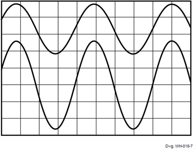
Figure 7. VOUT (upper) vs. IIN (lower) at 500 Hz
The phase shift becomes quite noticeable with a 10 kHz input rate (figure 8), and very apparent at 20 kHz (figure 9). Note: Testing performed with 20 turns on a gapped toroid; and the voltage scales of the three plots are not identical. Other intermediate-frequency plots exhibit similar phase shifts, but were not included due to space limits. [Ed. Note: Limitations refer to the strictures of the original publication.]
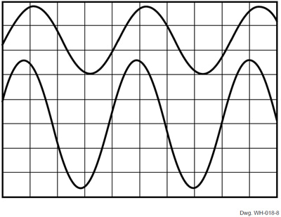
Figure 8. VOUT (upper) vs. IIN (lower) at 10 kHz
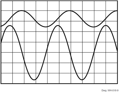
Figure 9. VOUT (upper) vs. IIN (lower) at 20 kHz
Also, it should be mentioned that this bandwidth limitation is correlated with the linear sensor IC. The magnetics (and induced coupling) is definitely not a restricting factor to bandwidth within this range of operating frequencies.
Obviously, with such bandwidth limitations, Hall sensor ICs cannot sense high-power PWM circuitry exploiting power MOSFETs or IGBTs at normal, inaudible operating frequencies (>20 kHz), but a linear HED is viable for DC and 'mains' power.
Linear HED Response to Application of Power − Increasingly, systems designers confront stringent power 'budgets,' and seek techniques to conserve current and power. Battery-powered and battery 'backup' designs are particular concerns, and any method capable of curtailing power is scrutinized.
A recurring technique is to (periodically) activate the sensor IC circuitry by switching the power supply on for brief intervals, and then off for longer periods. Average power is related to duty cycle. Thus, for low duty-cycle applications, the power consumed can be decreased substantially. Fixed-voltage IC regulators (with an ENABLE input) are one very viable circuit technique to switch the HED supply and reduce average power.
Clearly, the time required for a linear Hall IC to provide a stable, usable signal is very important, and two different linear HEDs were evaluated to ascertain their power-up response characteristics. The devices exhibit dissimilar properties, and the oscilloscope plots portray their dynamic operation upon applying power to the linears. These plots include a 5% window to compare the settling of the signals as the voltage attains its final value.
The latest linear HEDs (with dynamic quadrature offset cancellation) have a slower response than an earlier generation that exploits the orthogonal Hall element. The previous series (A3506, etc.) settles to above 95% of final voltage in less than 1 ms (per figure 10), and takes approximately 15 ms (per figure 11) to reach its final value. The very obvious tradeoff: speed vs. accuracy and resolution of the signal voltage at power-up.
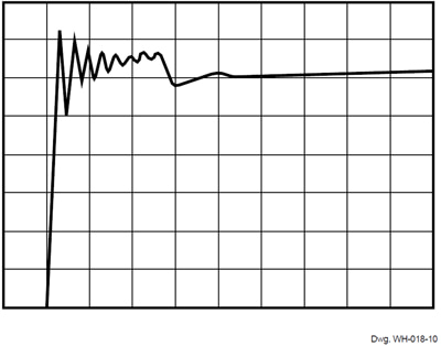
Figure 10. A3506 Power-Up (0.2 µs/div.)
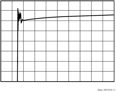
Figure 11. A3506 Power-Up (2.0 µs/div.)
The newest devices (A3515 and A3516) exhibit a slower response (≈ 25 µs to ≥95%, and ≈ 40 µs for a final, stable voltage level). These plots reveal basic tradeoffs in performance vs. response speed, and the latent potential for conserving power.
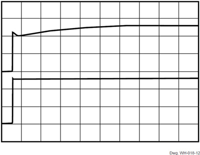
Figure 12. A3515 Power-Up (5.0 µs/div.)
Linear Hall Sensor Device/Toroid Hysteresis − Tests executed at ±6 A, which induce a substantial output voltage signal swing, reveal that any error involving hysteresis is rather minor (≈ 1% for the combination of linear HED (A3516) and gapped toroid). Inherently, linear Hall sensor ICs exhibit no hysteresis. However, different slotted toroids (and varied magnetic materials) may possess differing hysteretic properties.
The actual measured voltage differentials ranged from ≈ 16 mV to ≈ 22 mV with >2.1 V changes. Hysteresis is a minor concern when using ferrite cores, but other ferrous cores (such as powdered iron) may exhibit different characteristics.
Thus, a complete, thorough evaluation of specific toroids and the associated linear sensor IC would be a very prudent (and recommended) suggestion.
Core (Toroid) Saturation − Normally, the saturation of a core should not be an issue. A current-sensor application design that employs sufficient turns to drive the output voltage of the HED to nearly full scale (at the maximum design current) first induces saturation of the sensor IC. For optimum accuracy, the number of turns used should induce output voltage transitions that (just) fall short of saturating the sensor IC (more on this).
Zero Crossover − With a linear Hall-effect sensor IC, zero crossover corresponds to a zero magnetic field (no induced flux field as B = 0 with 0 A). The HED output voltage with a zero magnetic field equates to 1 ⁄ 2 supply (i.e., the quiescent output voltage).
Wide-Band Output Noise of Linear HEDs − The wide-band noise of these linear Hall ICs is inconsequential, and its value linked to the device chosen. The testing specifications for the recent, stable linear Hall IC series are:
- B = 0
- BW = 10 Hz to 10 kHz
- I OUT ≤1 mA
Typical equivalent input noise voltage (Vn) values for the two series of linears are:
- A3506, A3507, A3508: 125 mV
- A3515, A3516: 400 mV
Given that the lowest sensitivity of these HEDs is 2.5 mV/G, plus that accurate measurement is not feasible at very low flux strengths (more on this later), the consequences of wide-band noise is (typically) a very minor consideration. Other factors (particularly quiescent output voltage drift with temperature) are much more significant.
The System Temperature − A crucial constituent to consider, the temperature range must be well understood, properly specified (without inordinate margins), and controlling this very vital design element greatly aids the ability to realize reasonable accuracy. Note: Open-loop designs cannot (easily) resolve small variations in current. A core hysteresis of ≈ 1% precludes this without contemplating the other (and more acute) effects of temperature upon a linear HED output parameters and their relationship to performance.
Quiescent Output Voltage (DC Offset) − Essentially, the DC offset of a ratiometric, linear Hall IC relates to its deviation from the nominal quiescent output voltage (i.e., 1 ⁄ 2 supply). Lacking a system calibration or individual 'look-up' table, this DC parameter very tangibly affects accuracy of any current-sensing system utilizing linear Hall ICs. By referring back to both figures 3 and 4, and tables 2 and 3, the significance of DC offset (V OQ , or quiescent output voltage) is very plain.
The latest ratiometric Hall-effect sensor ICs specify the DC quiescent output voltage limits as 1 ⁄ 2 supply ±0.2 V [Ed. Note: Refer to Addendum.]. The quiescent output voltage drift over the HED operating-temperature range corresponds to ±10 gauss with the newest linear Hall ICs.
A significant facet of the static quiescent voltage is its tolerance limits. Present specifications list ±0.2 V [Ed. Note: Refer to Addendum.] from the nominal, and this translates into a ±8% maximum error without any temperature-induced effects (A3515/3516). Obviously, this latent error factor poses a formidable constraint, and must be given serious deliberation if accurate voltages are prerequisite to system performance.
DC compensation for the quiescent output voltage is feasible by regulating the supply to achieve the 2.5 V nominal, but this also influences sensitivity and any interrelated offsets are likely to prove intolerable in production. Per figures 3 and 4, boosting the supply offsets a low quiescent output voltage, and reducing the supply compensates for a high quiescent voltage. However, such offsets adversely influence sensitivity and counteract the positive aspects of 'nulling' the quiescent voltage.
Because the sensitivity specifications for the newest linears encompass a ±10% tolerance without any temperature effects, 'nulling' the quiescent output voltage (to 2.5 V) to escape a ±8% error in the quiescent output voltage seems rather absurd.
The DC drift of the earlier linears equated to ±20 gauss for the 'premium' type, and ranged to ±50 gauss for a 'limited' temperature unit. Also, the ranges of tolerances for quiescent output voltage of prior ICs was broader (or very much broader) than the newest ICs with offset cancellation.
This impedes the capacity to design an accurate, precise linear sensing system that operates over a broad temperature range. Designs necessitating tight current-sensing tolerances must confront and reconcile any concerns linked to quiescent output voltage (value and drift), and these are discussed in greater detail in the section Accuracy of Open-Loop Linear Hall Sensor ICs.
Applying the drift relationships mentioned above, the maximum quiescent output voltage drift error can be closely approximated. These calculations are based upon the (nominal) linear sensitivities:
- A3515: ±10 G × 5.0 mV/G ≈ ±50 mV
- A3516: ±10 G × 2.5 mV/G ≈ ±25 mV
- A3506: ±20 G × 2.5 mV/G ≈ ±50 mV
- A3507: ±35 G × 2.5 mV/G ≈ ±87 mV
- A3508: ±50 G × 2.5 mV/G ≈ ±125 mV
Essentially, the list establishes the A3516 as the favored linear when the quiescent voltage drift is an important criteria, and maximum sensitivity is not the primary consideration. In current-sensing applications this entails twice the number of turns (vs. A3515) to attain the same voltage swing.
Over a full-scale voltage swing (≥±2.0 V) the maximum error with the A3516 is ≤±1.3% but, consistently, quiescent voltage drift is <±3 G (≈ ±7.5 mV with the A3516). This error factor is dependent upon temperature; hence, sufficient turns should be employed to drive the output near full-scale. This minimizes the overall effect of temperature-related quiescent output voltage drift. Therefore, operation near full-range is absolutely advised as the ΔVOQ error percentage is lower.
Temperature Influence upon Sensor IC Sensitivity − The nominal sensitivities (and ranges) of both of the new linears was mentioned previously. However, the circuit tolerances were unspecified. The ICs have different nominal sensitivities; however, the temperature-related maximum shifts are identical. Reiterating sensitivity and range, plus adding the tolerances, produces the following Hall-effect IC parameters and device temperature shifts:
- A3515: Sensitivity, 5.0 mV/G ±10%
- ΔSensitivity (ΔT) at TA= Max, -2.5% (min), +2.5% (typ), +7.5% (max)
- ΔSensitivity (ΔT) at TA= Min, -9.0% (min), -1.3% (typ), +1.0% (max)
- Magnetic Range, ≥±400 G (≥±2.0 V)
- A3516: Sensitivity, 2.5 mV/G ±10%
- ΔSensitivity(ΔT) at TA= Max, -2.5% (min), +2.5% (typ), +7.5% (max)
- ΔSensitivity(ΔT) at TA= Min, -9.0% (min), -1.3% (typ), +1.0% (max)
- Magnetic Range, ≥±800 G (≥±2.0 V)
- Temperature Ranges:
- TA(min), -40°C
- TA(max), 85°C or 125°C
Essentially, the attainable accuracy of open-loop linear HEDs involves DC offset and sensitivity.
Accuracy of Open-Loop Linear Hall Sensor ICs − In any classic mystery, at this juncture the 'plot' thickens. Because precise, exacting measurement demands are increasing, a concise explanation of the interrelated elements associated with attaining 'accuracy' and dependability is next. Accuracy, repeatability, cost, etc. are very interrelated.
Though parametric maximums can be defined, the cumulative impact on accuracy is quite nebulous. Also, it is improbable that all worst-case errors occur coincidentally. Increasingly, cost-sensitive designs are based upon typical specifications, and this may precipitate a small (although tolerable) failure rate that cannot (easily) be decreased.
Pinpointing the absolute accuracy of 'open-loop' current sensing is beyond this treatise. However, reviewing the essential factors supports analysis.
- Hysteresis, hys, ≈ ±1%
- Output Quiescent Voltage, VOQ, ±8% [Ed. Note: Refer to Addendum.]
- A3515 or A3516: 2.5 V ±0.2 V
- Output Quiescent Voltage Drift, ΔVOQ, ±10 G
- A3515: ≤±50 mV
- A3516: ≤±25 mV
- Sensitivity at TA = Max, ±10%
- A3515: 5.0 mV/G
- A3516: 2.5 mV/G
- ΔSensitivity at
- TA = Max, -2.5% to +7.5%
- TA = Min, -9.0% to +1.0%
- Positive/Negative Linearity, ≈ 99.7%
- Symmetry, ≈ 99.7%
- Wide-Band Noise, en, 400 µV
Clearly, some of these elements are very crucial to attaining accurate current sensing, while others are rather inconsequential. Fundamentally, errors correlated to hysteresis, linearity, symmetry, and wide-band noise become quite insignificant. The factors linked to quiescent voltage and sensitivity are (absolutely) essential to any implementation of an accurate and precise current sensing design.
Errors linked to quiescent output voltage drift are range dependent and device related. The ±10 G (typically <±5 G) shift correlates to a potential error of 50% with a 10 gauss applied magnetic field. However, the ±10 G drift represents less than 1.5% with a field strength >667 G. Thus, the quiescent voltage error factor is 'non-linear' and is (substantially) diminished with large output-voltage swings of the A3516 linear HED.
The quiescent output-voltage tolerance is listed as a percentage (≤±8% [Ed. Note: refer to Addendum.]). This is predicated upon a nominal ratiometric (1 ⁄ 2 supply = 2.5 V), and the specified limits of ≤±0.2 V [Ed. Note: Refer to Addendum.]. Because the majority of linear Hall sensor ICs are much closer to nominal (≤±0.1 V), the ±8% tolerance represents a very 'worst-case' quiescent output-voltage scenario.
The sensitivity parameters also pose considerable error potential. However, these listings equate to a worst-case analysis. Further, the relationships between sensitivity and the effects of temperature are not (as yet) completely specified. Whether a consistent correlation between devices near either limit of sensitivity and temperature-induced shifts exists is not specified. The temperature-related effects might be nil, or miniscule (temperature cancels any cumulative deviations), or cumulative (temperature further exacerbates the tolerances).
Based upon the published parameters and limits, open-loop current-sensing designs cannot readily expect to attain results below ≈ ±10% to ±15%. However, after reviewing recent plots based upon test data (A3515/16), the prospect for boosting the measurement accuracy (absolutely) improves.
Two plots (figures 13 and 15) delineate VOQ vs. temperature. The +25°C data register an A3515 minimum of 2.468 V; a maximum of 2.512 V; the A3516 spans from a minimum of 2.464 V to a maximum of 2.501 V. This is much tighter than specified. The -3 sigma limits for the ICs are: 2.457 V (A3515), and 2.462 V (A3516). The +3 sigma data limits are 2.520 V (A3515) and 2.509 V (A3516), and these voltages convert to well within the published ±8% tolerances [Ed. Note: Refer to Addendum.] for the quiescent output voltage of these linears.
Data for the A3515 provides the following:
| VOQ in volts with VCC = 5 V |
||||
|---|---|---|---|---|
| Ambient Temperature | −40°C | 25°C | 85°C | 150°C |
| -3 σ | 2.448 | 2.457 | 2.463 | 2.472 |
| min | 2.461 | 2.468 | 2.473 | 2.481 |
| mean | 2.487 | 2.489 | 2.493 | 2.501 |
| max | 2.517 | 2.512 | 2.520 | 2.530 |
| +3 σ | 2.525 | 2.520 | 2.523 | 2.531 |
| VOQ in volts as a percentage drift from value at 25°C |
||||
|---|---|---|---|---|
| Ambient Temperature | −40°C | 25°C | 85°C | 150°C |
| -3 σ | -4.04 | 0.00 | -1.15 | -1.54 |
| min | -2.90 | 0.00 | -0.60 | -0.60 |
| mean | -0.59 | 0.00 | 0.74 | 2.38 |
| max | 2.60 | 0.00 | 2.40 | 5.50 |
| +3 σ | 2.86 | 0.00 | 2.63 | 6.31 |
Data for the A3516 provides the following:
| VOQ in volts with VCC = 5 V |
||||
|---|---|---|---|---|
| Ambient Temperature | −40°C | 25°C | 85°C | 150°C |
| -3 σ | 2.454 | 2.462 | 2.462 | 2.466 |
| min | 2.458 | 2.464 | 2.467 | 2.472 |
| mean | 2.484 | 2.485 | 2.483 | 2.485 |
| max | 2.503 | 2.501 | 2.498 | 2.499 |
| +3 σ | 2.514 | 2.509 | 2.504 | 2.504 |
| VOQ in volts as a percentage drift from value at 25°C |
||||
|---|---|---|---|---|
| Ambient Temperature | −40°C | 25°C | 85°C | 150°C |
| -3 σ | -3.97 | 0.00 | -3.36 | -5.13 |
| min | -3.60 | 0.00 | -1.60 | -2.90 |
| mean | 0.12 | 0.00 | -0.14 | 0.56 |
| max | 3.20 | 0.00 | 3.08 | 5.70 |
| +3 σ | 4.22 | 0.00 | 3.60 | 6.25 |
The data and plots of ΔVOQ vs. temperature also record better performance than the specified limit of ±10% (earlier listed in millivolts). Figures 14 and 16 show the VOQ drift is well within range, and the drift is very small in any narrow temperature band about +25°C. Clearly, temperature range affects the output voltage shift tolerances.
Because these plots and data entail characteristics that fall within certain HED specifications, some earnest deliberation on the achievable accuracy is absolutely advised (particularly if the temperature range is limited). Fundamentally, the effects of temperature are the foremost consideration in any endeavor to attain single-digit (<10%) precision without calibration and/or compensation methods.
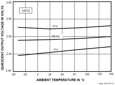
Figure 13. VOQ vs. Temperature (A3515)
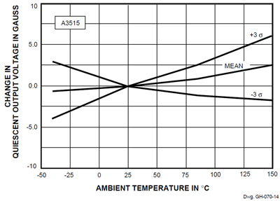
Figure 14. ΔVOQ vs. Temperature (A3515)
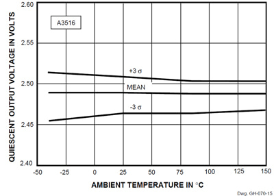
Figure 15. VOQ vs. Temperature (A3516)
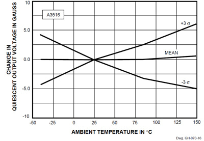
Figure 16. ΔVOQ vs. Temperature (A3516)
Effects of Sensitivity upon Accuracy − The plots and data for sensitivity confirm that the new linear HEDs are within published limits, and delineate another (albeit secondary) constituent in the resolution of accuracy. The device sensitivity and its interrelated variation over temperature are conservative, albeit without extreme test margins. Figures 17 through 20 depict the sensitivity data.
Data for the A3515 provides the following:
| Sensitivity in mV/G | ||||
|---|---|---|---|---|
| Ambient Temperature | −40°C | 25°C | 85°C | 150°C |
| -3 σ | 4.408 | 4.683 | 4.795 | 4.842 |
| min | 4.454 | 4.793 | 4.930 | 4.927 |
| mean | 4.761 | 4.988 | 5.109 | 5.121 |
| max | 5.181 | 5.316 | 5.392 | 5.359 |
| +3 σ | 5.113 | 5.293 | 5.423 | 5.400 |
| Sensitivity as a percentage drift from value at 25°C |
||||
|---|---|---|---|---|
| Ambient Temperature | −40°C | 25°C | 85°C | 150°C |
| -3 σ | -7.6 | 0.0 | -0.1 | -0.7 |
| min | -7.1 | 0.0 | -0.9 | -1.0 |
| mean | -4.7 | 0.0 | 2.3 | 2.5 |
| max | -2.5 | 0.0 | 3.7 | 4.4 |
| +3 σ | -1.9 | 0.0 | 4.6 | 5.8 |
Data on the A3516 reveals similar properties:
| Sensitivity in mV/G | ||||
|---|---|---|---|---|
| Ambient Temperature | −40°C | 25°C | 85°C | 150°C |
| -3 σ | 2.174 | 2.313 | 2.393 | 2.410 |
| min | 2.263 | 2.401 | 2.465 | 2.476 |
| mean | 2.340 | 2.457 | 2.530 | 2.528 |
| max | 2.586 | 2.700 | 2.758 | 2.728 |
| +3 σ | 2.506 | 2.600 | 2.667 | 2.646 |
| Sensitivity as a percentage drift from value at 25°C |
||||
|---|---|---|---|---|
| Ambient Temperature | −40°C | 25°C | 85°C | 150°C |
| -3 σ | -7.1 | 0.0 | 1.1 | -0.1 |
| min | -6.8 | 0.0 | 2.0 | 0.9 |
| mean | -5.0 | 0.0 | 2.7 | 2.6 |
| max | -4.0 | 0.0 | 3.7 | 4.3 |
| +3 σ | -2.9 | 0.0 | 4.2 | 5.3 |
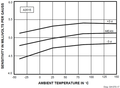
Figure 17. Sensitivity vs. Temperature (A3515)
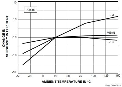
Figure 18. ΔSensitivity vs. Temperature (A3515)
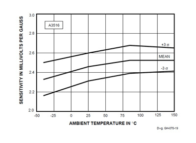
Figure 19. Sensitivity vs. Temperature (A3516)
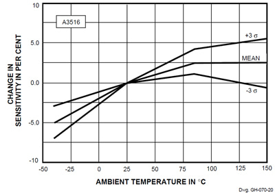
Figure 20. ΔSensitivity vs. Temperature (A3516)
Clearly, neither data nor plots reflect the overall distribution of the ratiometric linear Hall sensor ICs. This insight into accuracy is intended to advise of a basic necessity to reconcile the attainable limits of precise current sensing with HEDs, but it does not imply any definite constraint. Ultimately, the application of innovative, thoughtful circuit-design techniques determines the essential limits of open-loop Hall-effect current sensing.
Calibration and Compensation − Current-sensing designs endeavoring to realize an open-loop accuracy below ±10% should consider alternatives. Implementing 'hardware' calibration and/or compensation represents a costly, complex option, and (for most designs) should be ignored.
Whereas it is very feasible to establish trip points by using a comparator (or multiple comparators) calibrating, or compensating, for temperature and quiescent voltage to realize a full range of linear operation is a formidable task. The comparators can provide discrete current signals (overcurrent, normal operation, etc.) with useful accuracy, but cannot (easily) distinguish small current changes.
Increasingly, software is the solution to extending the accuracy of HED current sensing. Typically, this involves microcontrollers, µPs, or computers, and a software calibration/ compensation scheme.
Because the linearity, symmetry, and ratiometry of linear HEDs is ≈ 100%, these error factors can (largely) be disregarded. The temperature range is a definite factor if the system requires a wide operating range. However, a benign environment with a narrow temperature span alleviates design difficulties. The use of software (and a µC/µP) to exploit a look-up table necessitates measuring and storing sufficient data points to implement an acceptable (and individual) calibration technique for each current sensor IC. This (usually) involves the following calibration/compensation steps:
- Measuring and storing VOQ (the null current),
- Measuring and storing (specific) current points,
- Computing sensitivity from VOQ and data, and
- Measuring/storing temperature drift (if needed).
Determining the current level involves employing the 'look-up' data to calculate the current value via using the stored VOQ and sensitivity data.
- Measure VOUT and calculate current value, and
- Measure system temperature and compensate for its drift effects (if a system requirement).
In essence, the 'look-up' table corresponds to the 'calibrated' linear HEDs already mentioned. This software/look-up table method can easily achieve <±10% accuracy, and its ultimate limit (perhaps ≈ ±1%) is probably constrained by factors linked to software development, the requisite calibration and compensation (including equipment), and the associated costs and time of increased accuracy.
Obviously, the data-storage demands non-volatile memory for the parametric measurements, and an individual, initial calibration program. A look-up table compensates for the variations in quiescent voltage, sensitivity, and temperature effects. The latent errors associated with these constituents to system accuracy can be minimized by a software calibration and compensation technique. Although this may appear to be complicated and costly, the other solutions are liable to be more complex and more expensive than using a low-cost 8-bit µC.
Sorting of Hall-Effect Sensor ICs − Although this approach could tighten device output parameters; presently, only linears with published datasheet limits are available for sale. Some 'value-added' sorting is provided by others, but this procedure and service is neither common nor inexpensive. Despite this, specific customers have elected to solve formidable design issues by outside testing, sorting, and selecting linear HEDs to specific, tightened device limits. Clearly, any improvement in availability of presorted HED ICs is a definite advantage to current-sensing designs, and the availability of 'sorted' HEDs may change.
Size and Form of Sensor Assembly − Because various sizes of toroids with slots expressly cut to fit a HED package are available (Eastern Components, Inc.), a typical size cannot be identified. Figure 21 illustrates one basic configuration that is provided in six different current ranges (peak current ratings sensed are: 1 A, 3 A, 5 A, 8 A, 10 A, and 100 A). The length, height, and width vary somewhat, and the largest version measures 0.950" long, 1.025" high, and 0.500" wide; all versions are PCB through-hole form.
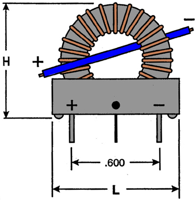
Figure 21. Hall IC Current-Sensing Assembly
Cost of a Current-Sensing 'Sub-System' − Identifying the costs associated with a linear Hall IC-based current sensor is virtually as difficult as the various issues involved with system accuracy. The costs of the indispensable components (linear HED and slotted toroid) can readily be determined, and the prices of the complete assembly depicted in figure 21 start at ≈ $8.00 (1000 quantity). [Ed. Note: Valuations in 1997 USD.]
Slotted ferrite cores (usually) cost <$1.00 (even in modest quantities), and the linear Hall-effect sensor IC costs range from <$2.50 to <$3.25 (1 k pieces). This price span reflects the various Hall-sensor IC types and the different temperature ranges. Obviously, unit costs diminish in higher volumes, and the combined sensor IC/toroid cost could easily fall (well) below $3.00 for volume production. A conversion from ferrite cores to powdered iron toroids with a `cast` gap can meaningfully reduce overall cost. Rather than ferrites with an $0.80 to $0.85 cost, powdered-iron cores are estimated to be ≈ $0.20 to $0.25 in similar quantities.
However, other factors such as engineering time, software programming, assembly labor, etc. vary (considerably) based upon each individual design requirement. Clearly, every system temperature, resolution, and accuracy are prerequisites that affect the system cost. The outlays of developing and implementing a high-resolution, very precise design with a wide temperature range are greatly different than sensing only excessive current. An overcurrent fault detection application may allow a very broad tolerance (perhaps ±20%), and this would not warrant any of the software 'look-up', stringent device and temperature evaluation that a precise, full temperature design mandates.
Therefore, only the essential components (and the assembly of figure 21) can be identified. Costs associated with software creation, system design engineering, etc. are (well) outside the realm of utilizing linear Hall ICs for current sensing.
Protecting High-Power Electronics
A classic example of current-sensing detection and protection for high-power IGBTs is shown in figure 22. This diagram can relate to a single-phase of an adjustable speed drive (ASD) for an AC induction motor or other power circuitry that requires a full-bridge or triple half-bridge drive (for example, a 3-phase PM brushless DC motor). Such a configuration can detect excessive current in the supply rail (upper current sensor). This can result from shorting the power rail to ground, or a shorted output combined with a corrresponding IGBT that is activated. Any combination of either a shorted lower or upper output with an on output in the opposite portion of the same 'leg' can result in an (unsafe) overcurrent fault in the system.
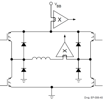
Figure 22. ‘Full-Bridge’ with Current Sensor ICs
Alternatively, the linear sensor IC in series with the winding (center sensor) provides detection from shorted loads, and also monitors the actual coil current. Current sensor ICs in both locations should preclude fire and safety hazards (and protect any personnel); and high-speed 'shut-down' circuitry can prevent damage to the power outputs (if the overcurrent results from an external fault such as improper equipment servicing). Clearly, overall circuit response speed (shutdown time) is critical to protecting the system and providing safety.
Summary and Perspective
The applications for linear Hall-effect sensor ICs in open-loop current sensing continue to evolve and expand. Presently, the devices available are far superior to any earlier linears, and advancements in design, processing, packaging, testing, etc. are incessant and relentless. As mentioned, present-day HEDs have tolerances and temperature drifts that pose formidable challenges to those intending to design, develop, and implement systems that demand dependable, single-digit accuracy over a wide range of system operating temperatures.
Expect further progress in HED performance and temperature stability, more functional integration, and other developments that make linear HEDs more viable for higher resolution current sensing.
Future linears may allow programming the sensor IC after HED packaging. This would permit users to tune the gain (sensitivity), calibrate the output quiescent voltage (VOQ), and compensate for the issues of temperature variations. Clearly, this involves an innovative, more complex technique in the circuit design and testing. However, the opportunities for applying such Hall sensor ICs expand exponentially.
Hall-effect sensor ICs have undergone revolutionary changes since their integration in the late 1960s. With further advancements and improvements, the applications for new linear HEDs are expected to expand and multiply to satisfy the many emerging needs of future power electronics systems.
Acknowledgement
The symbol for a linear Hall-effect current sensor [Ed. Note: As used in figure 22. The Χ mark is standard for indicating magnetic actuation.] was created by Raymond Dewey [formerly] of Allegro MicroSystems. Presently, no standard or accepted schematic symbol exists for current sensors utilizing Hall-effect technology.
References
Course: P. Emerald, "Open-Loop Current Sensing for Power Conversion and Motion System Applications" in Principles of Current Sensing, PCIM Power Electronics Institute, Chapter six, PowerSystems World '97; Baltimore, MD; plus various contributors of the chapters comprising this one-day professional advancement course.
Workshop: P. Emerald and Joe Gilbert "Integrated Hall-Effect Sensors for Motion Control and Positioning Applications," PowerSystems World '95, Long Beach, CA.
Addendum
Since this paper was written (December 1997), and presented, the A3515 and A3516 ratiometric, linear Hall-effect sensor ICs have been superceded by the A132x series. Information on the newer series is available on the Allegro website, at A1324-5-6.
Also, after the original publication, a change to the specifications for the A3515 and A3516 ratiometric, linear Hall-effect sensor ICs was made. In April 1998, the new, and tightened, limits for quiescent output voltage were changed from the original 2.5 V ±0.2 V to 2.5 V ±0.075 V. In addition to this upgrade in the quiescent output voltage limits, the effective linear current range can be extended by widening the toroid gap (i.e., slot) to 'desensitize' the magnetic coupling.
Per the section titled Quiescent Output Voltage (DC Offset), originally, the specifications listed the ratiometric output as (nominally) 2.5 V. The limits were 2.3 V (min) and 2.7 V (max) with VCC = 5 V over the device operating temperature range. This improvement affects the achievable accuracy of systems applying the ratiometric, linear Hall-effect sensor ICs (refer to the section that is titled Accuracy of Open- Loop Linear Hall Sensor ICs.
As mentioned, this paper shows the following output quiescent voltage limits:
VOQ .................................. 2.48 V to 2.52 V (±8%)
The upgraded specification now shows this as:
VOQ .............................. 2.425 V to 2.575 V (±3%)
This tightened specification significantly enhances the ability to realize more accurate measurements via utilizing these linear, ratiometric Hall-effect sensor ICs. This means that single-digit accuracy is a reality for some designs (especially those with limited temperature fluctuations).
Linear Current Range(s) − Per the original material (page 5) on Linear Current Range, with 'tight' magnetic coupling (»60 mil gap to match the sensor package) the ranges are unchanged:
A3515: ≥±400 G ÷ 6.9 G/A » ±58 A
A3516: ≥±800 G ÷ 6.9 G/A » ±116 A
'Desensitizing' the magnetic coupling can readily be realized via expanding (widening) the slot in the toroid. The first endeavor to desensitize the magnetic coupling involved increasing the slot to 3 mm (≈ twice the package body), and this reduced the flux coupling and increased the upper current limit as follows:
A3516: ≥±800 G ÷ 3.85 G/A » ±210 A
Testing revealed that placement of the sensor IC case had no effect upon the magnetic coupling. Centering the 'calibrated' linear Hall-effect sensor IC case resulted in the same output signal as positioning the case against either face of the slot. Because many users endeavor to attain higher current ranges, another evaluation ensued (after new ferrite toroids were obtained from Eastern Components, Inc.).
The next extension of the current range limit was undertaken with toroids gapped at 6 mm (e.g., more than 4× the package thickness dimension). This (very) 'desensitized' magnetic coupling increased the maximum current limit per the following calculation:
A3516: ≥±800 G ÷ 1.7 G/A » ±470 A
Further evaluations are intended as toroids gapped with differing dimensions become available. This should offer a more complete, albeit overlapping, set of current ranges with an upper limit (as yet) unknown. Also, other toroid materials (powdered iron in particular) are to be evaluated.
Summary
The tightened quiescent output voltage tolerance offers better accuracy for the ratiometric, linear HEDs, and widening the toroid slot increases the maximum current limitation of these devices.
This paper was presented at the International Appliance Technical Conference, Ohio State University, May 6, 1998. Reprinted by permission.
STP98-1