Recent Trends in Hall-Effect Current Sensing
By John Cummings, Michael C. Doogue, Andreas P. Friedrich
Abstract
This paper presents recent advances in integrated Hall-effect–based current sensor ICs. It covers the various packaging concepts for integrating the primary current path into the system, the major improvements in IC parameters, as well as a few examples of typical application circuits for uninterruptible power supplies (UPS), inverters, and battery monitoring.
Introduction
The demand for low-cost, accurate, small-size current sensor solutions has grown rapidly during the last decade, in industrial, automotive, commercial, and communications systems. Various technologies can be used to transduce an electric current to a proportional voltage. The advantages of a Hall-effect magnetic detector are the inherent voltage isolation from the current path and the integration of the Hall element and interface electronics on a single silicon chip.[1] New design concepts and the systematic use of advanced BiCMOS technology have allowed further improvements in IC performance. These also have opened the door to new product approaches by supporting the integration of additional functions, such as power protection, in the same current sensor IC. This paper covers the basic packaging and IC design concepts of the Allegro™ ACS current sensor IC family and explores some recent trends that have enabled Allegro to develop its next generation of fully integrated low-cost current sensor devices.
Packaging Concept
Allegro current sensor IC devices are characterized by the integration of a monolithic linear Hall IC and a low-resistance primary current conduction path into a single-shot overmolded package. Device accuracy is optimized through the close proximity and precise positioning of the Hall transducer relative to the copper conductor. Low power losses and high voltage isolation are intrinsic to the packaging concept. The final size, shape, and additional components of the packaged current measurement systems depend on the amplitude of primary current to be measured. This sections details the innovative packaging technologies for different current measurement ranges.
Currents up to 20 A
For small nominal currents, up to ±20 A, the Hall die and the primary current path are packaged in a standard-footprint SOIC8 surface mount package, shown in figure 1 and figure 3. This provides a compact, low profile solution that is compatible with high volume automated board assembly techniques. The use of flip-chip technology allows an optimized magnetic coupling between the active face of the Hall element and the magnetic field generated by the current being sensed. A flux concentrator is therefore not required. The internal resistance of the copper path used for current sensing is typically 1.5 mΩ for low power loss. The power terminals are also electrically isolated from the low voltage signal I/O pins. Careful IC and package design permitted further improvement of the voltage isolation of the device, with a typical DC isolation voltage of 5 kV, and an rms isolation voltage of 1.6 kV minimum and 2.5 kV typical (at 60 Hz for 1 minute) between primary current path and signal sides.
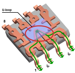
Figure 1. Internal structure of an ACS package, showing the U-shaped primary copper conductor and the single flip-chip–mounted Hall IC.
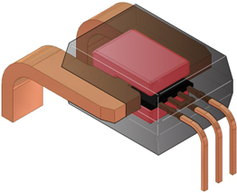
Figure 2. Internal structure of the CB package, showing the primary conductor (copper, left), the flux concentrator (red) and the linear sip Hall ic (black) and signal pins (copper, right).
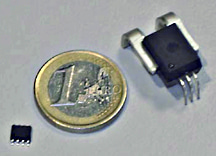
Figure 3. Photograph of ±20 A (LC package) and ±200 A (CB package) current sensor ICs, shown with a coin for comparison.
Currents up to 200 A
For higher currents, the cross section of the copper conductor has to be increased to accommodate the current density within the material, which is provided in the CB package. Because of the magnetic coupling between this thicker conductor and the linear Hall element, a flux concentrator has to be used. The copper path, linear SIP Hall device, and concentrator are precisely assembled before being overmolded. Through careful design of the system, the primary conductor resistance is typically as low as 100 µΩ and a minimum rms isolation voltage of 3 kV (at 60 Hz for 1 minute) is achieved between primary path and signal sides. Figure 2 shows the internal structure of such a ±200 A current sensor, and figure 3 shows a photograph of both this and the ±20 A package types.
Currents Above 200 A
If currents to be measured are higher than 200 A, the ICs can be used in a current divider configuration.[2] This method involves splitting the path of the current being sensed. The simplest approach is to design a notched bus bar such that only a well-controlled fraction of the current flows through the device, the other going through a shunt path (see figure 4). The current split ratio is determined by the geometry of the bus bar. An inherent disadvantage of this approach is that it reduces the current resolution by the same proportion as the current is divided.
The resolution of the current sensing system can be increased if the current is split equally and two devices are used in parallel (see figure 5). A simple circuit involving level-shifting and adding the outputs of the two devices can be used to obtain a linear output proportional to the total primary current.[2]
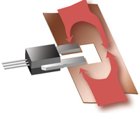
Figure 4. Current divider configuration. The current sensor IC can be connected directly to a bus bar.
Figure 5. Equal current splitting with enhanced resolution. The outputs of the two devices can be combined to obtain a linear output proportional to the total current to be sensed.
IC Design
This section details the basic chip architecture and most important IC parameters.
Block Diagram The central element of the device is a precise, low-offset silicon Hall IC. A block diagram is shown in figure 6. The magnetic flux generated by the primary current affects the Hall element. A BiCMOS chopper stabilization circuit is utilized to reduce signal offset and to stabilize the output of the IC over its operating temperature range.[3] The on-chip electronics produce an analog voltage that is proportional to the input current.
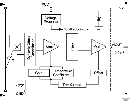
Figure 6. Block diagram of the circuit.
The output is ratiometric, which means that both the offset and sensitivity scale with VCC. Device accuracy is optimized through end-of-line trimming of the offset, sensitivity, and temperature response. The ICs are designed to measure both positive and negative currents, but the parameters can be trimmed for uni-directionality if required. The device is trimmed after packaging in order to reduce package stress effects on the Hall element. As shown in figure 6, an external bypass capacitor is recommended, to reduce noise. If the bandwidth of the application allows it, a simple rc filter can be used at the output to further improve signal-to-noise ratio.
±20 A Model Main Features Although the SOIC8 devices are designed for ±20 A, they can withstand large transient overcurrents of up to 100 A. The limiting factor determining the overcurrent capability of the devices is the junction temperature of the IC (TJ(max), which equals 165°C), and is therefore determined by the thermal design of the printed circuit board (PCB) in the application.
The main features and benefits are summarized as follows:
-
AC and DC current measurement
-
1.5 mΩ internal conductor resistance
-
1600 VRMS (min) isolation voltage
-
4.5 to 5.5 V supply operation
-
50 kHz bandwidth
-
±1.5% total output error at room temperature
-
operating temperature range of –40°C to 85°C
-
small footprint, low-profile SOIC8 package
-
near-zero magnetic hysteresis
-
ratiometric output from supply voltage
-
RoHS compliant (flip-chip high-temperature Pb-based solder balls are currently exempt from RoHS)
±200 A Model Main Features The thickness of the copper conductor allows survival of the device at up to 5× overcurrent conditions. The main features and benefits are summarized as follows:
- AC and DC current measurement
- 100 µΩ internal conductor resistance
- 3000 VRMS (min) isolation voltage
- 4.5 to 5.5 V supply operation
- 35 to 50 kHz bandwidth
- ±1.0% total output error at room temperature
- operating temperature range –40°C to 150°C (a function of primary current)
- small package size, easy mounting capability
- ratiometric output from supply voltage
- lead (Pb) free
Recent Trends
Current-sensing solutions for advanced industrial, automotive, commercial, and communications systems are facing new challenges. Although the solutions presented in the previous paragraphs are already covering a large variety of customer requirements, the general trend is clearly towards low cost, high accuracy, and small size systems, but with added functionality. This section describes two innovative devices developed at Allegro to address these needs.
Improved IC Performance In an effort to further improve the characteristics of the ±20 A low-profile SOIC8, Allegro developed a third generation device with specific focus on noise and total output error reduction. The chip design was developed on the latest Allegro low-noise 0.65 µm BiCMOS process (DABIC6). A total of 23 programming bits can be used to optimize following IC parameters after packaging:
- quiescent output voltage
- sensitivity
- sensitivity temperature coefficient
The combination of improved process performance, new design concepts, and additional programming capability resulted in a 2× reduction in noise. The total output error at IP = ±20 A was improved from ±8.4% to ±1.5% in an industrial temperature range, 40°C to 85°C.
This new device also has a filter pin that can be used to set the –3 dB point with a capacitor. This reduces the number of external components required to improve IC resolution (no sense resistor needed). The peak-to-peak current noise levels, for different filter capacitor values, at T = –40°C to 85°C, and IP = ±20 A, are given in the following table:
| Filter Pin External Capacitor (nF) |
Bandwidth (kHz) |
Peak-to-Peak Noise (mV (Typ.)) |
|---|---|---|
| 1 | 50 | 40 |
| 4.7 | 20 | 24 |
| 47 | 2 | 10 |
This new ACS712 device is a drop-in replacement of the previous generations, ACS704 and ACS706.
Added Functionality
For large volume applications, it may be worth integrating some additional functions on the Hall IC that would usually be realized with external components. In the implementation described below, this approach resulted in a new protection IC with integrated hot-swap gate driver and internal Hall-effect based element.
The block diagram of this ACS760 device is shown in figure 7. The power supply load is measured without the use of an external sense resistor. The part uses an integrated 1.5 mΩ copper conductor and a Hall-effect element to accurately measure load currents up to 30 A. The device contains overcurrent protection circuitry that trips at a user-selectable level between 30 and 40 A. If an overcurrent condition is detected, the fault output of the part trips and the gate of the external mosfet is pulled to ground. The delay between the detection of an overcurrent condition and gate shutdown is set by an external capacitor.
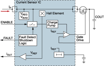
Figure 7. Block diagram of the protection IC with integrated hot-swap gate driver and internal 1.5 Ω Hall-effect based element.
Application Examples
This section gives two applications examples, in which the ACS devices support optimal current sensing solutions.
Battery Monitoring Smart battery systems require circuitry to monitor cell voltages, temperatures, and currents. For capacity monitoring applications, all of these measurements are critical. The most difficult to design-in properly, however, is current measurement. The reasons for this are the requirements for accuracy, power dissipation, and solution size.
Current measurement accuracy is essential to ensuring that the capacity monitoring algorithms are working well. The traditional method of measuring this current is with a shunt in the ground path or on the low side. The key problem with this method is that, to minimize I2R losses, the value of the shunt needs to remain very small. With this approach, low-current measurement accuracy becomes compromised. What it means for notebook computer applications is that during suspend, hibernate, or other low-power states, it is difficult for the battery to accurately monitor the current flowing into the system.
If the battery is using a 10 mΩ sense resistor to minimize power dissipation at nominal loads, when in a low-power state with only 50 mA of power draw, the voltage across the shunt would be only 500 pV. This voltage is very difficult to resolve, and complicated algorithms for estimating the residual capacity must be developed for the battery in order to compensate for this effect. These routines are conservative in nature, meaning that they tend to assume that the battery is losing a little more capacity than is actually calculated. The result can be an appearance of excessive loss in battery capacity over time.
Depending on the battery and the application, sense resistors in the range of 1 to 2 W would be required to monitor the currents. Typically in portable solutions, however, there is not enough space for 2 W resistors, so the solution is usually limited to 1 W resistors. For higher-current solutions, multiple resistors are used in parallel to keep the power ratings within the device limitations. Both solutions have a large impact on the board real estate required to fit these components.
By using a Hall-effect device as a shunt solution in the battery pack, the power dissipation in the pack can be reduced. The advantage of using Hall-effect devices is readily apparent with the low insertion loss of the device. In an SOIC8 package, the ACS712 lead-frame insertion loss is only 1.5 mΩ. The difference in power consumption over a range of load currents is shown in figure 8.
The use of a Hall-effect device as shown in figure 9 can increase the accuracy of current measurements. This block diagram shows a high current path and a low current path. The low-current path can be enabled for better accuracy at monitoring small currents. Not only does the solution shown in figure 9 provide higher accuracy for lower charge and discharge currents, but also it provides more signal than the shunt solution over the measurement range. Assuming that the Hall-effect device has a gain of 100 mV/A, this signal is much larger than the resulting signal across a shunt resistor, as shown below in figure 10.
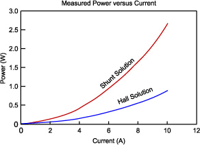
Figure 8. Power loss in shunt versus Hall-effect current sensing solutions.
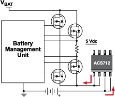
Figure 9. Improved accuracy and efficiency in battery monitoring with Hall-effect devices.
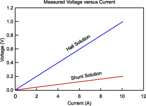
Figure 10. Output voltage of a Hall-effect solution compared to a 20 mΩ shunt.
The step increase in gain with the Hall-effect solution assumes that the application enables the high current path shown in figure 9. The actual threshold for the transition and level of hysteresis desired will be a function of the application as well as the value of the shunt employed.
The use of Hall-effect devices in battery systems will help to reduce the PCB area required for a shunt sensing solution and enable high-side sensing, which does not interrupt the ground path. The two major benefits in using a Hall-effect device are improving current measurement accuracy over a wider current range, and reducing power consumption by significantly reducing the 12R loss of the shunt.
Hall Effect Devices in UPS and Inverter Applications The use of either Hall-effect devices or current transformers (CT) is common in UPS systems. While CTs are seen as low-cost solutions, they actually require more support components than a Hall-effect solution and are strictly limited to ac applications. Another secondary cost attributed to using CTs to monitor the AC line voltage is the additional circuitry to manage the effects of inrush and possible core saturation during an inrush event.
UPS solutions require using the line voltage to charge a battery that is used to supply line voltage for a system in the event of a power failure. The goal of the UPS is to supply as much energy as possible with the maximum efficiency. For example, a 2200 VA UPS requires a typical 3-hour charge time. This same UPS can only supply approximately 24 minutes of power at half load (990 W) and 6.7 minutes at full load (1980 W). The input and output currents are monitored both for protection and to be able to show the battery state of charge with a level of confidence.
The ACS712 Hall-effect device is ideal for monitoring the input power or battery charge current for several reasons. The obvious benefit for a small form-factor Hall-effect solution is that the volume required is a fraction of the equivalent CT solution, and in addition there is an elimination of gain and additional protection components. The reason for this is that the ACS712 cannot overshoot the voltage on the isolated side of the device.
When powering the inverter stage at high loads, the optimal place to have the Hall-effect IC is at the line voltage itself to monitor the load currents directly. The reason is that the line voltage current may be as high as 15 to 20 ARMS, whereas the battery sourcing current may be in excess of 50 to 60 A, depending on the voltage of the battery stack and the efficiency of the converter. Below, figure 11 shows an example of using a Hall-effect device in a ups power train.
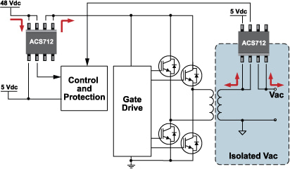
Figure 11. UPS power train architecture.
This next generation of Hall-effect devices is helping to resolve known issues with CTs and to improve the reliability of systems. By using Hall-effect devices in the battery charging system and inverter power train, the efficiency of the converters can be optimized. This can help to reduce the overall size of the system and save costs.
Conclusion
Innovative current sensing solutions for industrial, automotive, commercial, and communications systems were presented. The packaged devices consist of a low-resistance primary current path and a monolithic linear Hall-effect IC that integrates the Hall element and state-of-the art BiCMOS interface circuitry.
The devices cover a measurement range of up to ±200 A and can also be designed into higher current applications by using a current divider configuration. New approaches to address the trend towards low-cost, high accuracy, and small size current measurement systems with added functionality were detailed and two application examples presented.
Notes
- R.S. Popovic, "Hall Effect Devices", 2nd ed., IoP Publishing Ltd., 2004.
- R. Dickinson and A. P. Friedrich, Using Allegro Current Sensors in Current Divider Configurations for Extended Measurement Range, Allegro MicroSystems, LLC , applications note AN295036, April 2005.
- A. Bilotti, G. Monreal and R. Vig, "Monolithic Magnetic Hall Sensor Using Dynamic Quadrature Offset Cancellation," IEEE J. Solid-State Circuits 32, no. 6 (1997): 829-36.