A Micro-Packaged Linear Current Sensor IC
Primary conductor resistance of only 0.6 mΩ reduces power dissipation
By Shaun Milano
Allegro MicroSystems, LLC
The linear current sensor IC, the ACS711, is housed in a 0.75 mm thick low profile package measuring only 3 mm × 3 mm! It is designed for low-side and less than 100 V sensing applications requiring 5 A to 30 A continuous current sensing.
Traditionally, current sensing has been accomplished with sense resistors or current transformers that can take up a large PCB area. Sense resistor values from 10 to 50 mΩ can burn a significant amount of power at higher currents, which lowers overall system efficiency, while current transformers consume large PCB real estate. Hall-effect sensor ICs have been employed to provide a non-contact method of measuring current in conductors and to provide a voltage signal proportional to current flowing in conductors.
A new current sensor IC from Allegro™ MicroSystems, LLC, the ACS711 (figures 1 and 2) resolves the size issue with a truly small, 3 mm by 3 mm footprint with only 0.6 mΩ conductor resistance, which lowers power dissipation by an order of magnitude over typical sense resistor op-amp solutions. Full integration of the current sensor IC allows for factory programming at Allegro that delivers a solution that is more accurate while providing the additional benefits of small size and higher efficiency through reduced power loss in the current carrying conductor.

Figure 1. ACS711 QFN package size, in comparison to a U.S.
10-cent coin
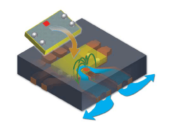
Figure 2. ACS711 device with QFN construction: yellow is the IC
chip, red is the Hall element, green lines represent magnetic flux,
and blue is the sensed current path
Packaging
Hall current sensor ICs with one turn and no magnetic core do not produce a large magnetic field, so placing the Hall sensing-element in close proximity to the sensed current is an attractive approach. The flux surrounding a conductor may be only a hundred gauss (10 mT) or less, and this diminishes rapidly with the distance of the Hall element from the conductor.
To optimize the performance, the ACS711 device employs an Allegro patented flip-chip magnetic field sensing technology, illustrated in figure 2. Flip-chip use allows the active area of the Hall transducer section of the IC (shown as the red square in figure 2) on the surface of the silicon to be placed in the closest proximity to the primary conductor. This allows for excellent signal coupling.
Classic flip-chip technology is employed, which makes the necessary connections to the signal circuit and supports the chip above the current conductor on the leadframe. The primary current path is efficiently channeled to the Hall element via a patented exposed current loop design, with terminations soldered directly to the PCB traces. With such close magnetic coupling to the conductor, signal sensitivity is maximized and the device can produce 90 mV/A and 45 mV/A for sensing 15 A and 31 A full-scale current, and the sensor IC requires only a 3.3 V supply.
Flip-chip technology also allows case molding plastic to fill the small spaces between the primary current carrying conductor and both the die surface and the device signal leads, providing galvanic (voltage) isolation. With the attractive small dimensions of this device, the package provides isolation only to supply voltage values below mains line voltage. The ACS711 has been optimized for low voltage circuits, < 100 V, such as: 48 V solar circuits, communications, and consumer electronics and audio applications. The device is also economical to assemble into finished products and is excellent for low-side sensing applications in residential and commercial white goods appliances and with general-use motor drivers.
Despite its small size, the ACS711 can sense relatively large currents in the QFN package, up to ±31 A. Sense resistor power dissipation is significant at higher current ranges and conducting such current levels in and out of IC packages has been a traditional limitation. The QFN package solves this issue with two large solder pads on the mounting surface and with careful detail to the shape of the primary sensed current conducting loop. The design uses substantial copper conductors within the package to form the sensed current loop, without bond wires. The primary conductor resistance in the QFN is only 0.6 mΩ, an order of magnitude less than most sense resistors employed in low-side sensing configurations. This reduces power consumption, and typical power dissipation at 30 A is only 0.54 W and at 15 A is just 0.135 W. This not only makes a contribution to system efficiency, but also allows the device to stay cool even at elevated currents. If customers prefer a leaded package for certain applications, a companion package, the SOIC-8, is also available for the ACS711 product. Please refer to the Allegro website at www.allegromicro.com for more linear current sensing ranges available.
Soldering and Thermal Characteristics
Notwithstanding the low power dissipation, an even lower thermal resistance to ambient than that inherently provided by the relatively small, 3 mm2 QFN package is required. Wide, highcurrent copper traces on the printed circuit board (PCB) are adequate to help cool the device, if designed properly. An example is shown in figure 3, the layout on the ACS711 prototyping board available from Allegro. Note that the two large pad areas, 4.5 mm across, are only slightly larger than the very small QFN package outline. On this board, two layers of 4 oz. copper are used, linked by thermal vias (those under the QFN can be filled or eliminated if necessary) to enhance thermal performance. The vias under the QFN can be filled or eliminated if necessary, as some customers find this difficult to accomplish in a production environment. Further design details and guidance for PCB mounting are available from Allegro.
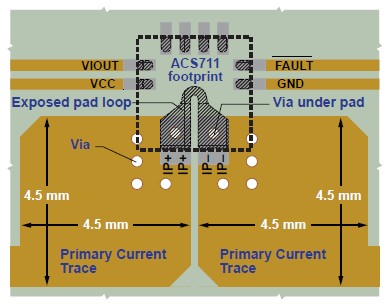
Figure 3. A PCB layout for the QFN current sensor IC (Allegro prototyping
board 85-0528)
Using the Allegro PCB of figure 3, temperature measurements were made across a range of sensed current levels. Figure 4 shows the results. The graph shows that at an ambient temperature of 85°C the sensor IC package can withstand 45 A continuous current before reaching the maximum recommended junction (die) temperature, 165°C. With proper PCB design, the device can be safely used in 30 A continuous-current applications at 85°C ambient temperature, with an approximately 50°C margin of safety before reaching a die temperature of 165°C.
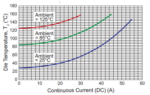
Figure 4. Thermal performance of the QFN mounted on the PCB
Device Features, Fault Output, and Accuracy
The voltage signal is dependent on the direction of the current flow, enabling measurement of bi-directional current flow, both AC and DC. At a zero-current level, the output voltage signal is half the supply voltage.
The ACS711 sensor IC also integrates a factory-programmed fast response digital fault output that has a 1.3 μs response time. It is set at 100% of the maximum current rating of the sensor IC. This fast fault signal can be used to prevent the destruction of IGBTs or other switching devices during short circuit or overcurrent conditions, or as a redundant fault feature in motor control applications.
Another inherent disadvantage of sense resistor with op-amp solutions is a reduction in accuracy with changes in temperature, because the sense resistor value changes. Hall-based sensor ICs are not subject to this error because the magnetic field generated by current flowing in a conductor is not temperature dependent. The Allegro ACS711 provides additional protection, against package thermal stress, through the application of an advanced Bi-CMOS process with built-in chopper circuitry to compensate for Hall element offset voltage changes. The fully integrated architecture of the ACS711 sensor IC further allows adjustment programming at Allegro end-of-line production testing to further reduce errors in gain and offset, delivering a more accurate sensing solution.
Summary
Advanced Allegro patented flip-chip packaging for linear Hall ICs has allowed the creation of a micro-sized, 3 mm × 3 mm fully integrated current sensor device, the Allegro MicroSystems ACS711, which has only 0.6 mΩ internal resistance, produced in a package that can really take the heat. Used with an appropriate PCB design, the device can be used for applications with over 30 A continuous current while reducing power consumption by an order of magnitude compared to existing sense resistor solutions.
Factory programming provides high accuracy in this IC, with an integrated fast response fault output. Together these techniques deliver the smallest current sensing footprint available for your application without compromising accuracy.
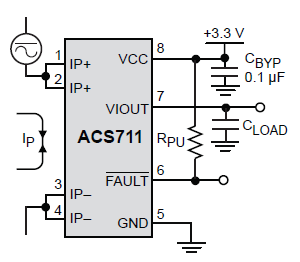
Figure 5. Typical application circuit for the ACS711
Based on an article originally published in Bodo’s Power Systems®, A Media, April 2013, pp. 36-38. Used with permission. For portions not copyrighted by original publisher, Copyright ©2013, Allegro MicroSystems, LLC
The information contained in this document does not constitute any representation, warranty, assurance, guaranty, or inducement by Allegro to the customer with respect to the subject matter of this document. The information being provided does not guarantee that a process based on this information will be reliable, or that Allegro has explored all of the possible failure modes. It is the customer’s responsibility to do sufficient qualification testing of the final product to insure that it is reliable and meets all design requirements.