Techniques to Minimize Common-Mode Field Interference When Using Allegro Current Sensor ICs (ACS724 and ACS780)
By Evan Shorman,
Allegro MicroSystems, LLC
Introduction
Allegro MicroSystems current sensor ICs can be divided into three main groups: sensors that need an external magnetic core, sensors that have a core built into the package, and sensors that have an integrated current-carrying loop but no core. Among the latter group are sensors that have common-mode field rejection (CMR) capabilities. This application note will discuss the mechanism of CMR and focus on how to best use this mechanism through optimized circuit board design and layout.
Background
In ICs using an integrated current-carrying loop, the loop is designed to produce a magnetic field that can be measured by the IC. The magnetic field is translated into a voltage using the Hall effect. This Hall voltage is proportional to the magnitude and direction of current flow. Figure 1 is an example of how the magnetic field is produced by a specific current sensor IC leadframe. In the figure, the arrows show the current through the leadframe, and the color map describes the magnetic field generated when 100 A of DC current flows through the sensor. The source of the current was removed from the figure for clarity.
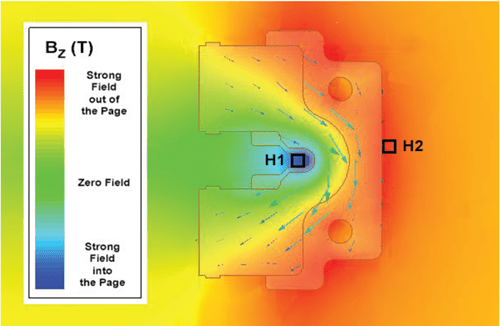
There are many advantages to using an IC with an integrated current-carrying loop: no need for a core, virtually no magnetic hysteresis, low power dissipation, and high accuracy over temperature. However, because the core is no longer present, the sensor is susceptible to stray magnetic fields generated by magnets or currents flowing in wires around the sensor IC. To combat the presence of stray magnetic fields, many of Allegro’s current sensors have a dual-Hall common-mode rejection scheme. The Hall plates are placed in such a way that the field sensed on each Hall plate is of opposite polarity when current is flowing through the IC’s integrated conductor or loop. In Figure 1, two Hall plate locations are denoted as H1 and H2. It can be observed from the figure that these two areas have magnetic fields that are opposite in direction.
This is the basic principle of the CMR techniques used: if the signals from the two Hall plates are subtracted, then the signals caused by the current in the integrated loop can be summed, and the common-mode (single polarity) signals coming from any stray magnetic fields incident on the IC can be rejected. For a simple example, assume that the magnetic field on each Hall plate, ±B, is equal but opposite; then:
H1 – H2 ∝ B1 – B2
B – B2 = B – (–B)
B – (–B) = 2 × B
Therefore,
H1 – H2 ∝ 2 × B
If it is assumed that there is an equal stray magnetic field, Bext, on both hall plates, then:
H1 – H2 ∝ B1 – B2
B1 – B2 = (B + Bext ) – (–B + Bext)
(B + Bext ) – (–B + Bext ) = 2 × B + Bext – Bext
2 × B + Bext – Bext = 2 × B
Therefore,
H1 – H2 ∝ 2 × B
In the application note, Common Mode Field Rejection in Coreless Hall-Effect Current Sensor ICs, the theory and governing equations of the CMR technique are covered in more detail. The main technique covered in this application note will be how to design and layout the current-carrying traces to these current sensor ICs. In addition, the application note provides guidance on minimizing other sources of stray fields.
Field from Nearby Current Path
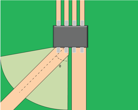
To best use the CMR capabilities of these devices, the circuit board containing the ICs should be designed to make the external magnetic fields on both Hall plates equal. This helps to minimize error due to external fields generated by the current-carrying PCB traces themselves. There are three main parameters for each current-carrying trace that determine the error that it will induce on an IC: distance from the IC, width of the current-carrying conductor, and the angle between it and the IC. Figure 2 shows an example of a current-carrying conductor routed near an IC. The distance between the device and the conductor, d, is the distance from the device center to the center of the conductor. The width of the current path is w. The angle between the device and the current path, θ, is defined as the angle between a straight line connecting the two Hall plates and a line perpendicular to the current path.
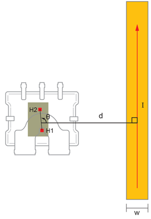
The position and orientation of the two Hall plates will vary between different ICs. For example, the ACS724 has its Hall plates rotated 90° from the Hall plates in the ACS780, as shown in Figure 3. When routing a current path near any Allegro current sensor IC with CMR, it is best to keep the angle θ as close to 90° as possible.
When it is not possible to keep θ close to 90°, the next best option is to keep the distance from the current path to the current sensor IC, d, as large as possible. Assuming that the current path is at the worst-case angle in relation to the IC, θ = 0° or 180°, the equation:
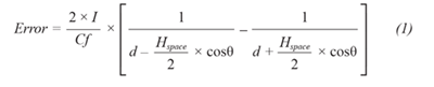
where Hspace is the distance between the two Hall plates and Cf is the coupling factor of the IC. This coupling factor varies between the different ICs. The ACS780 has a coupling factor of 5 to 5.5 G/A, whereas other Allegro ICs can range from 10 to 15 G/A.
Error Estimation
Equation 1 assumes an infinitely long, infinitely thin wire. It does not take into account the width or thickness of the current-carrying conductor. Figure 4 shows the error calculated for a current-carrying conductor passing the ACS780 in the worst-case direction (θ = 0° or 180°). The error was calculated using the idealized equation as well as a more computationally intensive set of equations that take the width and thickness of the conductor into account. The plots show that the calculated error is higher using the idealized equation. Therefore, Equation 1 can be used as a quick, conservative estimation of the error.
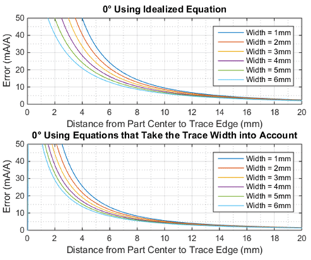
Using the more accurate calculation method, the error was calculated for different widths of the current path as well as different angles between the device and the current path. For all angles and widths, 4 oz. copper was assumed to set the trace thickness. The plots show that the width of the current-carrying conductor does play a role in the error, but the biggest factors are the angle to the device, θ, and the distance from the device, d.

Other Layout Practices to Consider
When laying out a board that contains an Allegro current sensor IC with CMR, the direction and proximity of all current-carrying paths are important, but they are not the only factors to consider when optimizing IC performance. Other sources of stray fields that can contribute to system error include traces that connect to the IC’s integrated current conductor, as well as the position of nearby permanent magnets.
The way that the circuit board connects to a current sensor IC must be planned with care. Common mistakes that can impact performance are:
- The angle of approach of the current path to the IP pins
- Extending the current trace too far beneath the IC
THE ANGLE OF APPROACH
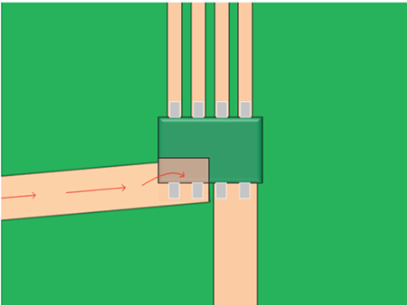
One common mistake when using an Allegro current sensor IC is to bring the current in from an undesirable angle. Figure 6 shows an example of the approach of the current traces to the IC (in this case, the ACS724). In this figure, traces are shown for IP+ and IP–. The light green region is the desired area of approach for the current trace going to IP+. This region is from 0° to 85°. This rule applies likewise for the IP– trace.
The limitation of this region is to prevent the current-carrying trace from contributing any stray field that can cause error on the IC output. When the current traces connected to IP are outside this region, they must be treated as discussed above (Field from a Nearby Current Path).
ENCROACHMENT UNDER THE IC
Another common mistake is to route the current trace too far beyond the IP pins. Depending on the device, this can cause two different problems. In the case of devices in SOIC and similar packages, this can cause stray fields to be generated onto the IC, causing a decrease in performance. In the LR package, with its larger and exposed IP bus, routing too far beneath the package can change the current path through the IP bus, thus altering the performance of the device. This effect on the LR package will be covered in more detail in the next section.
For the issue of stray fields, the problem is worsened when the current trace comes into the IP bus at an angle. When this happens, the current actually flows under the part, back towards the IP pins, and then up through the IP pins. This altered current path can cause stray fields to be generated that reduce the accuracy of the IC. This can be prevented by not allowing the current trace to the IP pins to encroach under the device.
EFFECTS OF A PERMANENT MAGNET
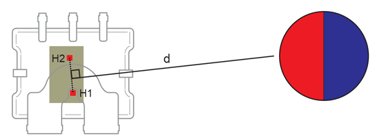
When a permanent magnet is in close proximity to a current sensor IC, the stray fields coming from the magnet can also impact the IC’s performance. In general, the stray fields coming from a magnet can vary greatly from magnet to magnet. It will depend on the magnet dimensions, material, magnetization direction, and many other factors. If the current sensor can be aligned such that the Hall plates are normal to the magnet (shown in Figure 8), the effect of these stray fields will be minimized.
Layout Practices Specific to the LR Package
ENCROACHMENT UNDER THE IC
In the LR package, the encroachment of the current-carrying trace under the device actually changes the path of the current flowing through the IP bus. This can cause a change in the coupling factor of the IP bus to the IC and can significantly reduce device performance.
Using ANSYS Maxwell Electromagnetic Suites, the current density and magnetic field generated from the current flow were simulated. In Figure 9, there are results from two different simulations. The first is the case where the current trace leading up to the IP bus terminates at the desired point. The second case is where the current trace encroaches far up the IP bus. The red arrows in both simulations represent the areas of high current density. In the simulation with no excess overlap, the red areas, and hence the current density, are very different from the simulation with the excess overlap. It was also observed that the field on H1 was larger when there was no excess overlap. This can be observed by the darker shade of blue.
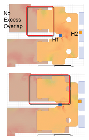
When the overlap is beyond what is recommended, other issues also arise—for example, a significantly reduced range for the angle of approach for the current. When the encroachment of the current trace onto the IP bus is too large, a dependency on approach angle develops, i.e. the angle of approach directly affects the coupling factor of the device. The best way to avoid this is by limiting the overlap of the current trace.
Conclusion
Allegro MicroSystems current sensor ICs have many advantages. They have near-zero magnetic hysteresis as well as a very low power dissipation. One disadvantage that comes with the lack of a core is a susceptibility to stray fields. However, many ICs have the ability to reject common-mode magnetic fields.
The CMR techniques work best when the common-mode field on both Hall plates is equal. Several techniques were discussed to minimize the difference in the common-mode field on the two Hall plates—how to route external current paths and other optimal layout techniques. When current paths cannot be routed in the most favorable direction, the estimation of the error was also presented. Some layout techniques were also discussed that are specific to the LR package, as it has characteristics that must be considered for optimum performance.
Overall, the techniques and calculations discussed in this paper will help customers to optimize Allegro current sensor IC performance.