
High-Side Vs. Low-Side Current Sensing: Why Placement Matters
Introduction
In the architecture of modern power electronics, achieving high accuracy and dynamic response is one part of the current sensing equation. As systems scale in power and complexity, from high-efficiency solar inverters and 800 V electric vehicle (EV) traction inverters to next-generation AI data center power delivery, the physical placement of the current sensor within the circuit topology becomes a foundational design parameter.
A system architect must determine where the sensor will reside relative to the load and the choice between low-side and high-side current sensing dictates the diagnostic capabilities of the system, the complexity of the control loop, and the fundamental safety and isolation requirements of the entire architecture.
This document is part of a comprehensive series that provides current sensor selection guidance to help engineers navigate the critical tradeoffs between sensor technologies. For additional content in this series, refer to Beyond the Datasheet: Mastering Current Sensing Selection.
What is Isolation and How Does Sensor Placement Affect It?
When selecting a current sensor, engineers often focus first on performance metrics like accuracy, bandwidth, and range. But for many applications, safety and isolation are the more critical design considerations, an accurate measurement is worthless if it cannot be captured safely. Capturing that measurement safely depends on a fundamental architectural concept: galvanic isolation.
Galvanic isolation is the design principle of physically and electrically separating two distinct domains of a circuit to prevent dangerous direct current flow between them, while still allowing data, signals, or power to be exchanged. In modern power electronics, isolation acts as the critical barrier between the lethal, high-voltage power stage and the sensitive, low-voltage control electronics (such as 3.3 V microcontrollers) and human operators.
It is not just a feature but a fundamental requirement that ensures the safety of users, protects sensitive downstream electronics, and enables robust, noise-immune system performance. The physical placement of a current sensor within a circuit topology and the sensor’s inherent isolation characteristics are foundational design decisions that impact system safety and performance.
The Three Topologies: Low-Side, High-Side, and In-Line Sensing
Current sensors can generally be placed in one of three locations relative to the load: the low side, the high side, or in-line with the load itself. Each placement subjects the sensor to a different common-mode voltage environment, which in turn defines the system’s isolation requirements, its fault-detection coverage, and the constraints it places on the control loop.
Low-side sensing places the sensor between the load and the system ground return, keeping its circuitry near ground potential at the cost of blind spots in fault detection. High-side sensing places the sensor between the positive power source and the load, giving it visibility into every fault current the source delivers, but exposing it to the full common-mode voltage of the power bus.
In-line (or phase) sensing places the sensor directly in series with the load itself, typically a motor phase, providing continuous current visibility independent of switching state, but subjecting the sensor to a common-mode voltage that swings between the DC bus and ground at the switching frequency.
Table 1 summarizes the key differences between each of the listed topologies and Figure 1 shows the sensor placement configurations for current sensing: low-side, high-side, and in-line motor phase sensing. The sections that follow examine each of these three topologies in turn, starting with the simplest and least demanding from an isolation standpoint: low-side sensing.
Table 5: Comparison of Low-Side, High-Side, and In-Line Current Sensing Topologies
| Attribute | Low-Side | High-Side | In-Line (In-Phase) |
|---|---|---|---|
| Sensor location relative to load | Between load and ground return | Between positive source and load | In series with the load (e.g., motor phase) |
| Common-mode voltage exposure | Near ground potential | Static, at full DC bus potential | Dynamic: swings between bus voltage and ground at PWM frequency |
| Galvanic isolation requirement | Not required | Mandatory | Mandatory, plus high CMTI |
| Short-to-ground fault detection | No, bypasses the shunt entirely | Yes, all source current passes through sensor | Yes, within the phase it monitors |
| Ground reference integrity | Disturbed ("ground bounce") | Undisturbed | Undisturbed |
| Duty-cycle / blanking-time impact | Limits max duty cycle at high switch on-time | None | None: continuous visibility regardless of PWM state |
| dV / dt / CMTI sensitivity | Low | Moderate (static common-mode, but fast edges during switching) | Highest: continuous exposure to full dV/dt at switching frequency |
| Relative cost & design complexity | Lowest | Moderate–high (isolation required) | Highest (isolation + CMTI) |
| Typical best-fit applications | Cost-sensitive, non-safety-critical designs | Safety-critical systems needing comprehensive fault coverage | FOC motor control, high-performance drives needing continuous phase current |
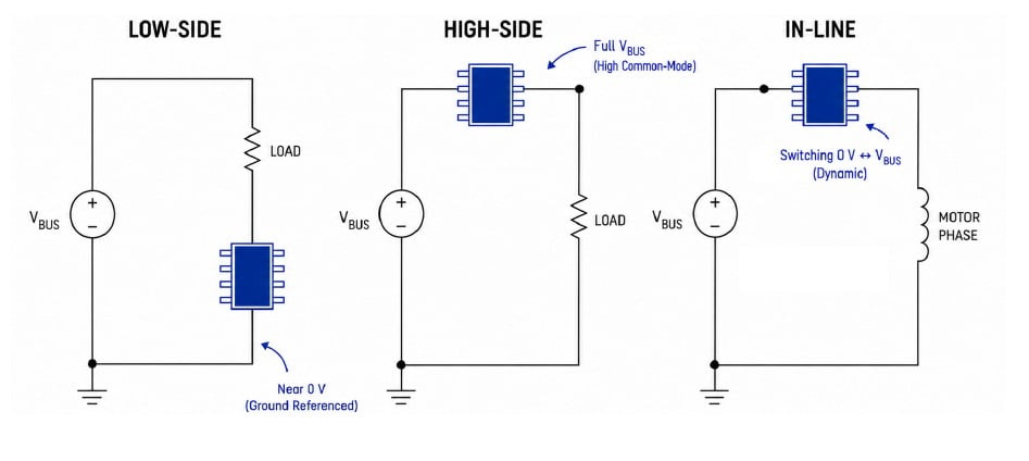
Figure 3: Sensor placement configurations for current sensing: low-side, high-side, and in-line motor phase sensing
Low-Side Sensing: Ground-Referenced Simplicity
In a low-side sensing configuration, the current measurement node is positioned between the load and the system ground return.
The primary advantage of low-side sensing is electrical simplicity. Because the sensor’s circuitry operates at or near ground potential, it is not subjected to the extreme common-mode voltages of the power bus, eliminating the need for high common-mode voltage rejection or robust galvanic isolation. This allows engineers to use simple, low-cost integrated options, like the ACS37041/ACS37042 and the ACS71240 in the EX package, to feed the analog-to-digital converter (ADC), typically at a lower total solution cost.
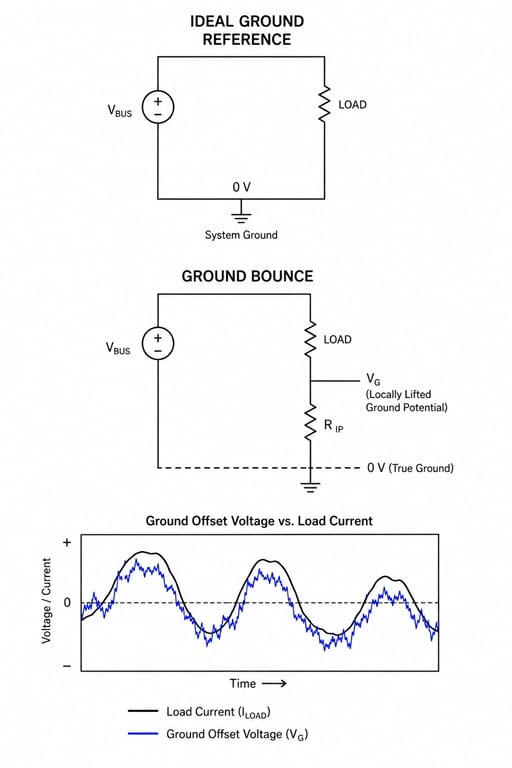
However, the physics of low-side placement introduce operational trade-offs that can reduce system stability and safety. Placing a resistive sensor in the return path lifts the ground potential of the load above the true system ground, causing an offset that dynamically fluctuates with the load current. This “ground bounce” degrades signal integrity and complicates control circuitry across the system. It degrades the signal-to-noise ratio (SNR) and causes referencing errors for microcontrollers, gate drivers, communication buses that share the same ground plane, or other ground-referenced systems.
In systems utilizing wide-bandgap semiconductors like Silicon Carbide (SiC) and Gallium Nitride (GaN), switching frequencies and edge rates are exceptionally high. Adding a shunt into the ground return path introduces parasitic inductance into the commutation loop. During high di/dt events, this parasitic inductance generates voltage spikes (V = L × di/dt) that can cause ringing, electromagnetic interference (EMI), and even false-triggering of the power switches.
Beyond hardware vulnerabilities, low-side sensing introduces significant software and control loop complexities in switching applications like motor drives. In a standard inverter topology, a low-side sensor can only measure the load current when the low-side power switches (MOSFETs or IGBTs) are turned on.
This creates a severe limitation: if the system requires a very high duty cycle (meaning the high-side switch is on most of the time), the low-side switch is only on for a brief fraction of the switching period. If this “on-time” is shorter than the settling time of the sensor and the downstream ADC, the system cannot accurately sample the current. Consequently, engineers are forced to artificially limit the maximum duty cycle of the inverter in software, which restricts the maximum voltage that can be applied to the motor, ultimately reducing the system’s peak mechanical power output and dynamic range.
The most critical flaw of low-side sensing is its inability to detect specific, catastrophic fault conditions. If the high side of the load shorts directly to the chassis or ground, a common failure mode caused by degraded motor winding insulation or mechanical damage, the fault current flows directly from the positive supply to ground, completely bypassing the low-side shunt. The system controller remains blind to current surges. Without visibility into this short-to-ground fault, protective overcurrent shutdown mechanisms cannot trigger, potentially resulting in hardware destruction.
High-Side Sensing: Diagnostic Superiority and the Isolation Mandate
To ensure comprehensive fault visibility and preserve true system ground, safety-critical systems overwhelmingly favor high-side current sensing. In this topology, the sensor is placed directly between the positive power source and the load. This is the preferred topology in most modern systems because it allows for comprehensive fault detection (short-to-ground) simplifying the overall system design, and it does not disturb the system’s ground reference. The sensor’s low voltage output must be galvanically isolated from the high bus voltage to protect the downstream microcontroller and ensure user safety.
High-side placement guarantees that all current leaving the source, including unexpected short-to-ground fault currents, must pass through the sensor. This allows the system to instantaneously detect and respond to any fault condition, including phase-to-phase shorts, in-line load faults, and short-to-ground events. Furthermore, because the sensor is removed from the return path, the system’s true ground reference remains undisturbed.
The need for isolation is driven primarily by the decision to place the current sensor on the high side of the load, between the positive power source and the load itself. The significant engineering challenge of high-side sensing lies in the voltage domain. The measurement node is now floating at the high potential of the system bus. This voltage, known as the common-mode voltage, can be anywhere from 12 V in a standard automotive system to 400 V, 800 V, 1000 V or even higher in electric vehicles and industrial applications. Figure 1 summaries the separation of the high-voltage current path from the low-voltage MCU while allowing the measurement signal to safely cross the isolation barrier.

Figure 1: Galvanic isolation separates the high-voltage current path from the low-voltage MCU while allowing the measurement signal to safely cross the isolation barrier
Table 1: Typical Common-Mode Voltage by Application and Recommended Sensing Topology
| Application | Typical Bus/Common-Mode Voltage [V] | Sensing Topology Typically Used |
|---|---|---|
| Standard 12 V automotive electronics | 12 | Low-side or high-side |
| 48 V mild-hybrid and e-bike systems | 48 | High-side |
| Industrial motor drives | 400-650 | High-side or in-line |
| EV/HEV traction inverters | 400-800 | High-side or in-line |
| Next-gen SiC/GaN EV & industrial systems | 800-1000 | High-side or in-line |
| AI data center power delivery | 800 | High-side |
To extract a precise current measurement and safely route that data back to a low-voltage microcontroller, the sensor must bridge this massive voltage differential. The sensor’s output signal must be read by a low-voltage component, such as a microcontroller operating at 3.3 V or 5 V. Without an electrical barrier between the high-voltage side and the low-voltage side, this massive common-mode voltage could damage the microcontroller and any other connected components.
In a high-side configuration, galvanic isolation ceases to be an optional feature and becomes a mandatory safety requirement. The isolation barrier must withstand continuous high working voltages to protect personnel and equipment, and it must simultaneously reject the high-speed voltage transients( high dV/dt) generated by fast-switching SiC and GaN power stages.
The Complexity of High-Side Shunt Applications
Attempting to use a traditional shunt resistor on the high side introduces severe architectural complexity. The small differential voltage generated across the shunt (ΔV = I × R) is now riding on top of a massive 800 V common-mode voltage. To safely extract this millivolt-level signal and route it to a 3.3 V or 5 V microcontroller, designers must deploy complex isolated amplifiers.
This introduces several engineering penalties:
- Isolated Power Requirements: The high-voltage side of the isolated amplifier requires its own isolated bias power supply to operate because the amplifier’s high-side circuitry floats at bus potential and cannot share the low-side supply rail. This necessitates additional DC-DC converters, transformers, and low-dropout regulators, inflating the Bill of Materials (BOM) and consuming valuable printed circuit board (PCB) footprint.
- Thermal Losses: Shunts operate via direct voltage drop, resulting in unavoidable I2R power losses that generate unwanted heat, lowering overall system efficiency.
- Vulnerability to High dV/dt: The physical footprint of a shunt and its associated isolated amplifier introduces significant common-mode capacitance. During the extreme voltage transients dV/dt generated by SiC/ GaN switching, this capacitance allows high-frequency noise to bridge the isolation barrier, corrupting the measurement signal or causing false fault trips.
Allegro’s ACS37200 addresses these penalties directly. By integrating an extremely low current-carrying conductor and 1097 VRMS certified basic isolation into a single surface-mount package, it replaces the shunt, isolated amplifier, and isolated bias supply chain described above with one factory calibrated device, reducing power loss and PCB footprint compared to a discrete, shunt-based implementation.
Table 2 summarizes this tradeoff in detail. Its industry-leading internal conductor resistance of just 50 μΩ reduces power loss compared to typical shunts, eliminating thermal bottlenecks in high-current paths up to ± 200 A. Combined with a 150 kHz analog bandwidth, a fast 4 μs response time, and an adjustable overcurrent fault output, the ACS37200 delivers high-efficiency, reliable, and space-saving high-side current sensing for demanding systems like electric vehicle (EV) onboard chargers, DC-DC converters, and solar inverters.
Table 2: High-Side Sensing Implementation Tradeoffs: Shunt + Isolated Amplifier vs. Integrated Magnetic Sensor
| Consideration | Shunt + Isolated Amplifier | Integrated Magnetic Sensor (Hall-Effect / TMR) |
|---|---|---|
| Isolation mechanism | External isolated amplifier IC | Inherent physical separation of conductor and die |
| Additional isolated bias supply required | Yes (DC-DC converter/transformer) | No |
| Power loss mechanism | I²R loss across shunt | Negligible resistive loss |
| BOM impact | Higher: shunt, isolated amp, isolated DC-DC, LDOs | Lower: single integrated device |
| PCB impact | Larger | Smaller |
| dV/dt / common-mode capacitance sensitivity | Higher: shunt + amplifier footprint couples noise across barrier | Lower |
| Design complexity | Higher | Lower |
Topology Redundancy
By placing sensors on both the high side (or in-line) and the low side of a phase leg, the system controller can perform real-time diagnostic cross-checking. According to Kirchhoff’s Current Law, the current entering the load must equal the current returning. If the high-side sensor reads 50 A, but the low-side sensor reads 0 A, the controller instantly identifies a catastrophic short-to-ground fault. If the difference is only a few milliamps, the system can detect subtle insulation degradation or leakage currents before a hard failure occurs. Table 3 summarizes fault detection coverage by sensor placement.
Resolving a leakage current of only a few milliamps against a background of tens or hundreds of amps places a premium on sensor accuracy. Allegro’s ACS71010 is factory-calibrated to a typical accuracy of 1% and integrates high-voltage isolation directly into the package, giving the redundant crosscheck the precision needed to distinguish genuine insulation degradation from ordinary measurement noise. Implementing this redundant topology safely and cost-effectively is impractical without the inherent galvanic isolation of integrated magnetic sensors on the high side, shunt-based alternatives reintroduce the isolated-amplifier penalties (BOM, thermal loss, dV/dt sensitivity) described above.
Table 3: Fault Detection Coverage by Sensor Placement
| Fault Type | Low-Side Only | High-Side Only | In-Line Only | High-Side and Low-Side (Redundant) |
|---|---|---|---|---|
| Short-to-ground (load positive to chassis) | Not detected | Detected | Detected (within monitored phase) | Detected, with cross-check confirmation |
| Phase-to-phase short | Not detected | Detected | Detected | Detected |
| Standard overcurrent | Detected | Detected | Detected | Detected |
| Insulation degradation/leakage current | Not detected | Not reliably distinguishable alone | Not reliably distinguishable alone | Detected (via KCL mismatch) |
| Ground-referenced noise/offset error | Present (ground bounce) | Not present | Not present | Not present |
In-Line (In-Phase) Current Sensing
While high-side sensing resolves the diagnostic blind spots of low-side placement, modern high-performance motor control algorithms, such as Field-Oriented Control (FOC), often drive architects toward a third placement option: In- Line (or Phase) current sensing. In this topology, the sensor is placed directly in series with the motor phases.
Unlike low-side sensors, which only see pulses of current depending on the switching states of the inverter legs, an inline sensor continuously measures the true phase current of the motor regardless of the PWM state. This continuous visibility completely eliminates the software blanking time issues and duty cycle limitations associated with low-side sensing, allowing the inverter to operate at much higher duty cycles, approaching the practical PWM limit, for maximum torque and power output.
While in-line sensing offers the most accurate representation of the load, it presents the most hostile environment for the sensor’s isolation barrier. The measurement node is no longer sitting at a static high DC voltage (like a high-side sensor) or near ground (like a low-side sensor). Instead, the common-mode voltage at the phase node is rapidly switching between the high-voltage DC bus and ground at the PWM switching frequency.
This exposes the sensor to continuous, extreme voltage transients (high dV/dt). Therefore, placing a sensor in-line mandates not only robust galvanic isolation to protect the low-voltage controller from the DC bus, but also exceptional Common-Mode Transient Immunity (CMTI) to prevent the high-frequency PWM switching noise from corrupting the sensitive analog output signal.
Allegro’s ACS37100 was engineered specifically for this environment. Built on Allegro’s XtremeSense™ Tunneling Magnetoresistance (TMR) technology, it delivers 10 MHz of bandwidth and a 50 ns response time, allowing it to track fast-edge PWM transitions at the phase node without the signal corruption or false trips that slower, less CMTI-robust sensors can experience in this application.
The Magnetic Advantage: Inherent Galvanic Isolation
To eliminate the cost, thermal losses, and complexity of high-side shunt applications, modern architectures rely heavily on integrated magnetic current sensors (utilizing Hall-effect or Tunneling Magnetoresistance (TMR) technologies).
Unlike shunts, magnetic sensors do not measure current via a direct voltage drop. Instead, they measure the magnetic field generated by the current flowing through a conductor, as defined by Ampère’s Law. Because magnetic fields pass freely through dielectric materials, the high-voltage primary conductor can be completely physically separated from the sensitive low-voltage semiconductor die.
This magnetic coupling provides inherent galvanic isolation. It allows the sensor to read the current accurately without any electrical connection to the high-voltage bus, entirely eliminating the need for secondary isolated amplifiers and dedicated bias power supplies. Establishing the necessity of high-side placement and the superiority of magnetic isolation naturally leads to the next architectural challenge: how is this physical barrier actually constructed within an integrated circuit?
Conclusion
The choice of where to place a current sensor is not a minor implementation detail, it is an architectural decision that contributes to each layer of the system, from the control algorithm down to the safety architecture.
Low-side sensing offers simplicity and low cost by keeping the measurement near ground potential, but that same ground-referenced placement leaves the system blind to short-to-ground faults, disturbs the ground plane under high di/dt switching, and imposes duty-cycle limitations that constrain motor performance.
High-side sensing resolves these diagnostic and ground integrity issues by placing the sensor where it can see all current leaving the source, but in doing so, it exposes the sensor to the full common-mode voltage of the power bus, making galvanic isolation a mandatory rather than optional design element.
In-line sensing extends this further, delivering continuous phase-current visibility for advanced control algorithms like Field-Oriented Control at the cost of subjecting the isolation barrier to the most demanding voltage transient environment of the three topologies.
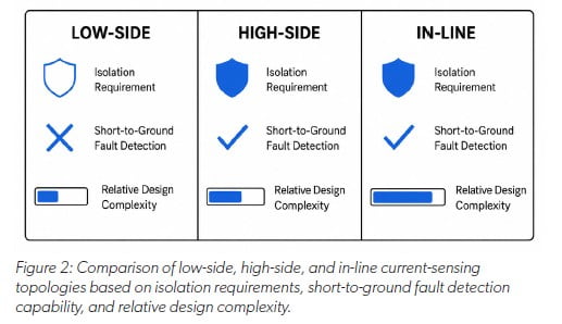
Across all three configurations, one requirement is constant: as systems move toward higher bus voltages, faster-switching wide-bandgap devices, and more stringent fault-detection and functional-safety requirements, the burden placed on the sensor’s isolation barrier only grows. Traditional shunt and- isolated-amplifier approaches can meet this burden, but only by adding significant cost, board area, thermal losses, and dV/dt vulnerability to the design. Integrated magnetic current sensors avoid these penalties by achieving isolation intrinsically, through the physical separation of the high-voltage conductor from the sensing die, rather than through additional isolation components layered onto a shunt-based signal chain. Figure 2 summarizes the three configurations while Table 4 offers a quick reference in selecting current sensor topology by design priority.
Understanding why a design needs isolation, and how much of it, is only the first half of the problem. The second half is understanding how that isolation is actually implemented and verified inside a sensor package, and how to specify it correctly for a given application’s safety.
The next segment of this series, Inside the Barrier: How Integrated Current Sensors Achieve Galvanic Isolation, will deconstruct the mechanics of package-level isolation, defining what specifications like working voltage, basic versus reinforced isolation, and creepage truly mean for system design, enabling safe, simple, and robust current sensing.
| Priority | Choice |
|---|---|
| Lowest cost, no short-to-ground detection needed | Low-side |
| Comprehensive fault coverage, safety-critical system | High-side |
| Continuous phase current for FOC / high-performance motor control | In-Line |
| Maximum fault diagnostics (including leakage detection) | High-side and low-side redundant topology |
This document is part of a comprehensive series that provides guidance about current sensor selection. For additional content in this series, refer to Beyond the Datasheet: Mastering Current Sensing Selection.