Short Duty Cycles Lead to Smaller DC-DC Converters
Introduction
This application note describes recent trends in the electronic component power management industry, in particular the innovative application of valley current mode control. It examines as an example the Allegro™ A4403 device, which provides this advanced form of power management.
Higher Frequencies Reduce the Size of Capacitors and Inductors
There is a continuing drive to shrink electronic solutions. This especially affects the DC-to-DC converter market, where there is more and more pressure to shift towards higher switching frequencies in an attempt to reduce the physical size and cost of key system-level components, such as the power inductor and filtering capacitors. This problem is demanding when generating very low output voltages and becomes even more challenging when combining with high input voltages.
To meet these requirements, DC-to-DC converter solutions must be able to generate very short duty cycles, or on-times, from the series MOSFET. Many of today’s switcher solutions, such as peak current mode control, are based on architectures that are over twenty years old, and which have fundamental design constraints in achieving very short on-times.
This article will describe a buck converter circuit that addresses the on-time limitation. It incorporates a new control architecture that implements valley current mode control, with userconfigurable on-time solutions.
Limitations of Today's Switcher Solutions
One of the most common control architectures used today is peak current mode control. While this control scheme has well documented benefits, it does suffer from a number of limitations.
One of the main problems of this scheme is that, when attempting to produce low output voltages from a relatively high switching frequency, the converter control loop cannot respond to the demanded switch on-time. Consequently the switcher has to operate in a region of pulse-skipping, or worse still, burst-mode, to obtain the correct output DC voltage. These modes of operation typically cause an excessive (AC) ripple voltage to appear on the output, which generally exceeds the specification requirements.
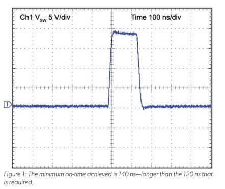
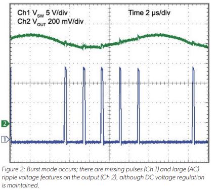
The waveforms in Figure 1 and Figure 2 illustrate a typical example of what can happen. They were produced under the following conditions: VIN = 18 V, VOUT = 0.8 V at 1.5 A, and Switching Frequency = 550 kHz. Under these conditions, the demanded on-time is 120 ns.
In this particular case, because peak current mode control cannot develop the required series switch on-time of 120 ns, the control loop misses some of the switching pulses in order to maintain the DC voltage regulation on the output. Missing these pulses results in the output voltage decreasing below the output target voltage. When the output voltage decreases below a certain level, the loop demands another switching pulse. But because of the lag effects caused by the control loop compensation components, rather than a single pulse occurring, a burst of several switching pulses occurs. This increases the output voltage beyond the target level. It can be observed that, although the output voltage is well regulated at 0.8 V from a DC point of view, the AC output ripple is more than 120 mV—some 100 mV more than it should be. This can mean a system-level problem for noise-sensitive circuits and for circuits that have undervoltage lockout protection schemes.
Peak Current Mode Operation
Peak current mode control works by sensing the current through the series switch and comparing this signal to the current-demand signal. The current-demand signal is set by the amplifier in the outer loop that monitors the output voltage. At the beginning of the switching cycle, the switch is turned on. The current through the switch is essentially the load current, plus a current ramp that increases through the period that the switch is on. Once the current ramp reaches the correct peak level, the on-time is terminated and the series switch is turned off until the next switching cycle is initiated.
The reason the on-time can be limited in peak current mode control schemes is that, when the switch initially turns on at the beginning of a switching cycle, there is an excessive voltage resonance in the circuit, caused by charging of the parasitic capacitor within the recirculation diode. This in turn can make the current sensing amplifier erroneously mistrigger, causing the current loop to behave in an unpredictable manner.
To ensure a legitimate peak current is detected, the current loop requires leading edge blanking. This blanking is typically set around a period of approximately 100 ns. This period, plus the response time of the current sense amplifier, can add a considerable delay, which has a direct impact on the minimum duty cycle that can be realized.
In the example of a 1 MHz converter operating from a 24 V supply and converting down to 0.8 V, the duty cycle required, D, can be calculated as:
D = (VOUT + VF)/(VIN + VF) = (0.8 + 0.35)/(18 + 0.35) = 0.063 or 6.3%,
where the Vf of the recirculation diode is 0.35 V. The required on-time, ton, is then:
ton = D/fSW = 0.63/(1 × 106) = 63 ns.
With an on-time of 63 ns, many peak current mode control solutions are unable to achieve the desired duty cycle. Consequently, the converters operate in either a pulse-skipping or burst-mode (as shown previously) to obtain the correct output DC voltage. These modes of operation typically create an excessive (AC) ripple voltage to appear on the output.
A Valley Current Mode Control Solution
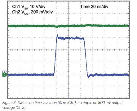
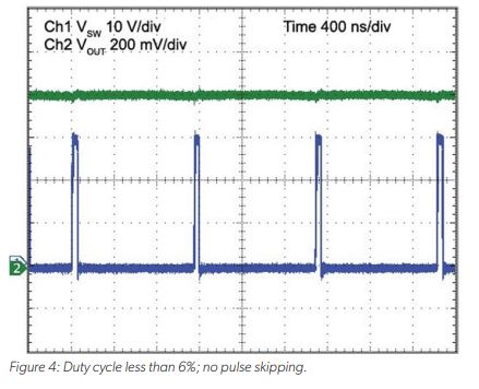
The Allegro A4403 provides a solution that avoids the aforementioned limitations, by a novel scheme using valley current mode control, along with a switch on-time that is determined by the input voltage. This technique allows on-times of less than 50 ns to be achieved. The waveforms shown in Figure 3 and Figure 4 were generated using a more extreme set-up than that used for Figure 1 and Figure 2, including an increased switching frequency of 1 MHz, an input voltage of 30 V, and the same output voltage of 0.8 V at 1.5 A.
Pulse Frequency Mode
It can be observed that, even with an input voltage of 30 V, the A4403 solution can easily convert down to 0.8 V with no pulse skipping and therefore no ripple appearing on the output. If a condition demands an on-time shorter than what the solution normally delivers, the A4403 will operate in a pulse frequency mode (PFM) of operation, reducing the switching frequency to an appropriate level.
This technique avoids the undesirable burst mode of operation. PFM operation produces excellent correction for load transients by adjusting the duty cycle and switching frequency according to the load variation. For example, during the transition phase, when changing from minimum to maximum load, the switching frequency increases, increasing the duty cycle and ensuring the charge into the load occurs more rapidly. Once the control loop is settled again under static conditions, the switching frequency remains constant. The schematic in Figure 5 illustrates this solution.
The resistor R1 sets the switch on-time duration. The ontime varies inversely with input voltage, ensuring a constant switching frequency (under static conditions). The minimum on-time period is determined by the response time of a single comparator and monostable, making it possible to achieve on-times of less than 50 ns. The valley current is sensed through an external resistor, R2, in the recirculation loop. In this case, when the series switch is off, the current through the recirculation loop decreases, and when it reaches the (valley) level set by the outer control loop, the series switch is commanded on. The blanking required in this position is minimal, as the relative parasitic components during the transition phase are much less than those experienced with peak current mode control.
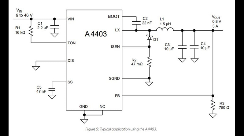
The current sense resistor can be a standard 1206 chip type, making it very low-cost. The fact that the resistor is external means that, for any given solution, the current limit is userconfigurable. Furthermore, the current limit is constant no matter the overload conditions. This is because compensation (which is required in peak current mode control schemes) is not necessary in this solution, so the currentdemand signal truly represents the condition of the load current.
Conclusion
Valley current mode control with configurable on-time is an effective, novel way of addressing many of the short-comings of peak current mode control. Valley current mode control schemes now can meet the demand for reduced-footprint electronic solutions because of advanced features incorporated in devices such as the Allegro A4403, which has fully integrated compensation for the control outer-loop, greatly simplifying the design-in process.
Originally published as: “Short duty cycles lead to smaller DC-DC converters,” Power Management: Design Line, February 25, 2005, < http://www.powermanagementdesignline.com/214502987>, accessed March 30, 2009. Portions not copyrighted by Power Management, Copyright©2005–2022, Allegro MicroSystems.
The information contained in this document does not constitute any representation, warranty, assurance, guaranty, or inducement by Allegro to the customer with respect to the subject matter of this document. The information being provided does not guarantee that a process based on this information will be reliable, or that Allegro has explored all of the possible failure modes. It is the customer’s responsibility to do sufficient qualification testing of the final product to ensure that it is reliable and meets all design requirements. Copies of this document are considered uncontrolled documents.