Breaking the Density Barrier: A Technical Deep Dive into Simplified SiC Gate Drive

In the relentless pursuit of higher performance for 800V electric vehicle systems, next-generation AI data centers, and grid-scale clean energy solutions, engineers are confronting a common, formidable obstacle: the power density wall. The core challenge has evolved beyond simply delivering more power; it's about delivering that power with maximum efficiency, within stringent physical footprints, and under demanding thermal constraints. As designers push the boundaries of performance, they consistently find that a significant contributor to this problem is the very architecture used to drive high-voltage Silicon Carbide (SiC) FETs. The conventional design methodology, which has served the industry for years, mandates a separate, isolated bias supply for the gate driver. While functional, this approach has become a critical bottleneck, forcing a cascade of undesirable design compromises. It inflates the bill of materials (BOM), complicates PCB layout with bulky magnetic components, and introduces significant sources of electromagnetic noise, ultimately undermining the primary goal of maximum power density.
This architectural complexity forces engineers into a difficult set of trade-offs. To accommodate the isolated supply, valuable board space must be sacrificed. The additional components, including a dedicated DC/DC converter and its associated transformer, not only increase cost but also create new challenges for thermal management and supply chain logistics. Furthermore, the larger current loops and parasitic capacitances inherent in these complex designs are a primary source of EMI, leading to countless hours spent in the lab troubleshooting, adding filtering, and implementing shielding to meet regulatory standards. The very component meant to unlock the power of SiC becomes a source of complexity that limits its potential.
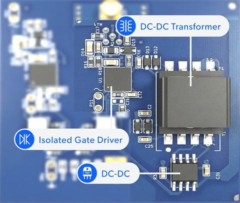
Figure 1. Gate drive architecture defines SiC system performance and board size
Allegro MicroSystems directly dismantles this long-standing barrier with a technically elegant and fundamentally different solution. We have solved this core design challenge in power conversion by creating a self-powered architecture that completely eliminates the need for external isolated bias supplies. This innovation is our patented Power-Thru™ technology, a paradigm shift that delivers the industry’s smallest solution footprint while drastically reducing the BOM. At its heart, the technology uses a recommended external mini-transformer, driven by the primary-side chip, to transfer both power and signals across a single, tiny magnetic isolation boundary. This elegantly simple approach removes the need for a dedicated, bulky DC/DC converter and its many associated components. The results are tangible and dramatic. In a real-world PFC Datacenter use case, this technology eliminates 25 components. In an automotive On-Board Charger (OBC), the savings are even more stark, with over 70 components removed from the design. This directly translates into a PCB size reduction of up to 50%, enabling engineers to build smaller, lighter, and more power-dense systems. Critically, this architecture also inherently improves noise performance by minimizing the size of the power transfer loop and reducing common-mode capacitance, a key factor in passing stringent EMI tests.
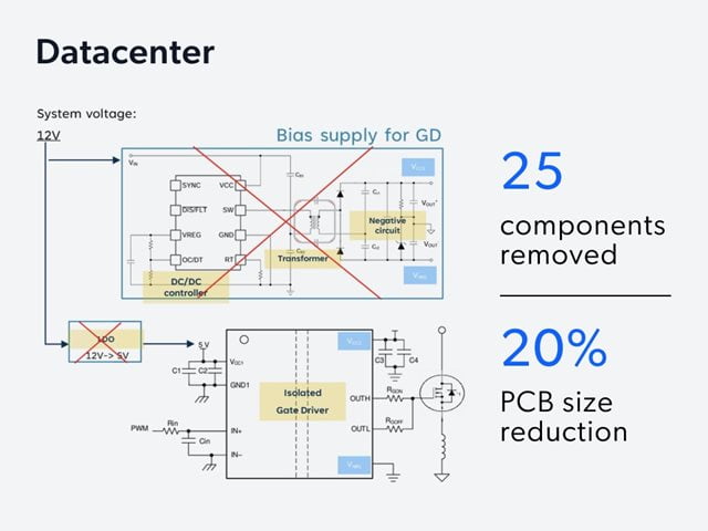
Figure 2. Allegro solutions reduce components and PCB size in data center designs
This industry-changing breakthrough is embodied in our new AEC-Q100 Grade 1 qualified AHV85003 and AHV85043 Isolated SiC Gate Driver Chipset. The technical features of this chipset are not arbitrary; they are precisely tailored to solve the most pressing high-voltage design challenges. To effectively switch modern SiC FETs with minimal switching losses, a key to system efficiency, the chipset provides a powerful gate drive with separate pull-up and pull-down pins capable of 6A source and sink current. This robust drive strength ensures fast, clean switching transitions even when driving FETs with a gate charge (Qg) up to 130nC.
Recognizing that flexibility is crucial for optimizing system performance and de-risking the supply chain, the chipset features a regulated bipolar drive. It offers selectable positive rails of 15V, 18V, or 20V and a configurable negative rail from 0V down to -5V. This allows designers to precisely fine-tune the gate voltage for a wide variety of SiC FETs from multiple vendors, enabling a robust multi-sourcing strategy without requiring a costly and time-consuming board redesign. The negative voltage capability is particularly vital for ensuring the SiC FET remains firmly off during high-noise events.
Furthermore, the Power-Thru architecture was engineered for exceptional reliability in the harshest electrical environments. It ensures stable operation in noisy, fast-switching applications with a Common-Mode Transient Immunity (CMTI) greater than 100 V/ns. This means the driver can withstand extreme voltage swings on the switch node without data corruption or unintended switching. To further enhance system robustness without adding external components, the solution also includes an integrated Active Miller Clamp. This critical feature provides a low-impedance path from the FET’s gate to its source during switching transitions, preventing parasitic Miller turn-on events caused by high dv/dt rates - a common and potentially destructive failure mode in half-bridge topologies.
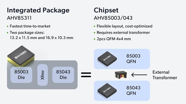
With Power-Thru, we provide a complete toolkit with two distinct implementation paths, empowering engineering teams to choose the strategy that best aligns with their project goals. The flagship AHV85311 integrated solution, which includes the isolation transformer within the package, provides a seamless, all-in-one route for accelerating time-to-market. It is a pre-validated, plug-and-play solution for teams who need to move quickly and focus their resources on system-level innovation. In contrast, the versatile new AHV85003/AHV85043 chipset empowers designers to optimize for cost and layout by selecting their own external transformer tailored for their specific isolation and form-factor needs. This path offers granular control for high-volume applications where every millimeter and every cent is critical. Both paths deliver the same game-changing efficiency, noise performance, and the freedom to use the SiC FETs of their choice.
Stop letting architectural complexity limit your power density and dictate your design cycle. The era of compromising on size, cost, and noise to drive high-voltage SiC is over. The 18V version of the AHV85003/043 chipset is available now, with 15V and 20V versions arriving in January 2026. Visit the Power-Thru Isolated Gate Driver page to explore our comprehensive design resources, including evaluation boards, datasheets, and application notes, and see how you can finally overcome the density barrier in your next high-voltage design.
Get the Full Technical Article
Download the complete "Breaking the Density Barrier" in PDF format to save for reference or share with your team.