PCB Ground Plane Optimization for Coreless Current Sensor Applications
Introduction
The ACS37610 is a Hall-plate-based differential current sensor designed to measure current flowing in a busbar or a PCB without using a ferromagnetic concentrator core. The ACS37610 is well-suited for electric vehicle applications (all-electric, hybrid, or plug-in), such as inverters, charging stations, on-board chargers, and DC links. This application note provides guidelines on how a PCB ground plane around the sensor location should be designed to achieve optimum performances.
The ACS37610 is a contactless current sensor and features differential sensing to reject common-mode stray magnetic fields. It is recommended for typical current measurement ranging from 200 A to more than 2000 A.
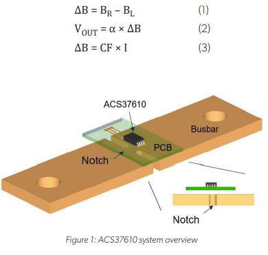
While the ACS37610 would function using any busbar design, in order to achieve the greatest performance (accuracy, high signal-to-noise ratio, high bandwidth, low sensitivity to mechanical tolerances, etc.), the busbar must include certain features. Some recommendations can be found in the Busbar Geometry and Design Techniques for Coreless Differential Current Sensors application note [1]. In that application note and as shown in Figure 1 of this application note, the ACS37610 is placed over a notch (or neckdown) in the busbar. This notch is intended to locally increase the current density and the signal measured by the IC.
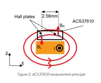
Figure 2 illustrates how the ACS37610 senses the magnetic field induced by the current I flowing in the busbar. The ACS37610 has two Hall plates sensitive along the Z axis and 2.58 mm away from each other. The left Hall plate measures the magnetic field BL, and the right Hall plate measures the magnetic field BR. The output of the sensor, VOUT, is proportional to the differential magnetic field, ΔB (equation 1 and equation 2). α is the ACS37610 output sensitivity to magnetic field. The relationship between the applied current and the differential field is given by the coupling factor, CF (equation 3).
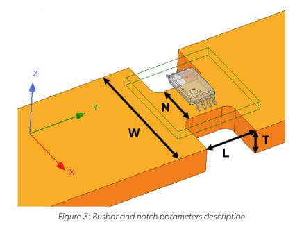
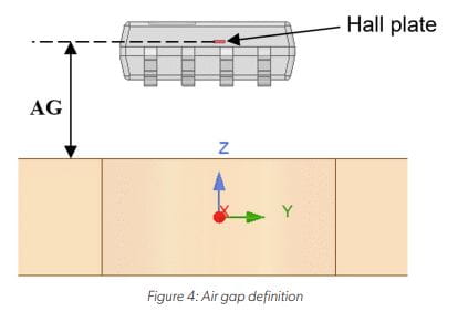
The notch dimensions are defined in Figure 3 and Figure 4. All conductors are considered made of copper. PCB layers are assumed to be 35 µm thick.
In this application note, the magnetic influence of the PCB ground (GND) plane on the current measurements is evaluated. A GND plane is usually used for the components connection to ground in order to reduce the return current path impedance and to protect against electromagnetic interference. However, when a primary AC current flows into a nearby conductor, eddy currents are induced in the ground plane. These eddy currents generate a magnetic field that can be sensed by the ACS37610 Hall plates: it leads to a primary current measurement error and/ or delay. This document also presents some counter measures to cancel the ground plane effect.
Note that all results in this document come from AC electromagnetic field simulations. Unless otherwise specified, the simulations are run with a sinusoidal primary current flowing into the busbar.
This application note focuses on the ACS37610, but the results also apply to any Allegro coreless current sensor family.
Busbar Reference Design
The Allegro busbar reference notch design is optimized for best DC, AC, and transient current performances. It is also designed for optimum thermal and mechanical behavior. The notch dimensions are N = 3 mm, L = 6 mm and T = 4 mm (cf. Figure 3). W = 18 mm is considered.
This reference busbar with notch is recommended for high primary current and high frequency applications such as inverters. While other busbar designs can be used, this application note uses the notch design as a reference to demonstrate the GND plane effect.
Ground Plane Effect
The PCB ground plane can be on any layer of the PCB. For these evaluations, it is assumed to be on the top layer (closest to the ACS37610).
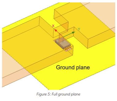
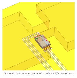
The case of a full ground plane is first simulated (Figure 5, ground plane in yellow). It gives the baseline of the ground plane influence. Another use case, with some cuts for the pin connections, is then evaluated (Figure 6). The cuts in the ground plane tend to prevent the eddy currents from flowing.
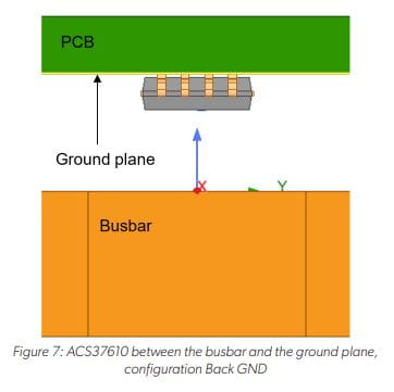
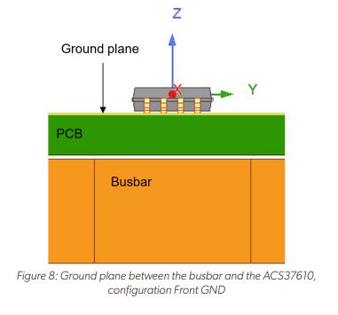
Two cases must be simulated: the first is with the ACS37610 in between the ground plane and the busbar (see Figure 7, configuration called “Back GND”) and the second is with the ground plane between the busbar and the ACS37610 (see Figure 8, configuration called “Front GND”). The air gap AG is held constant to AG = 2.5 mm in all the cases.
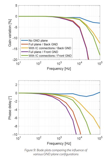
In Figure 9, these various configurations are compared over the input primary current frequency. One can notice that, without a GND plane, the reference busbar in conjunction with the ACS37610 has excellent AC performances up to at least 10 kHz.
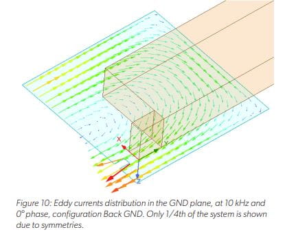
Compared to no GND plane, the full GND plane has a major negative impact on the AC performances, especially for the “Front GND” configuration. The eddy current can flow freely in the GND plane (Figure 10). In this case, the system can barely be used up to 1 kHz primary current.
As expected, the cuts in the GND plane for the IC connections improve the AC performances of the system. However, it might be insufficient, depending on the AC requirements.
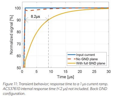
The ground plane would also affect the transient performances of some DC applications. For example, in the case of a surge, the response time of overcurrent detection can be significantly slowed due to the eddy currents in the GND plane. As illustrated in Figure 11, with a 1 µs ramp primary current driven in the busbar, the 90% response time is ~8 µs with a full GND plane, while it is <0.1 µs without the ground plane. These results do not include the response time of the ACS37610 itself (<2 µs) but emphasizes only the effect of the eddy currents in the ground plane.
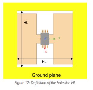
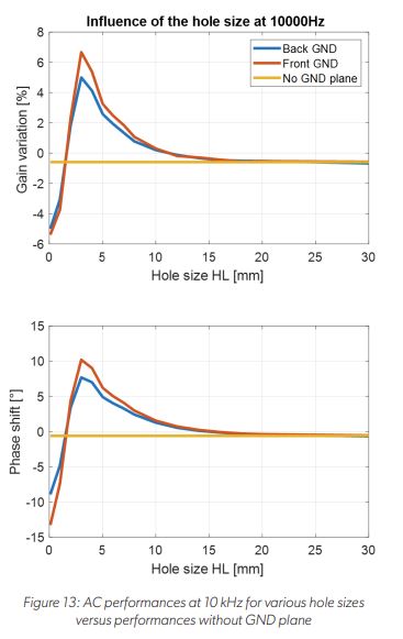
To reduce the influence of the GND plane on the AC performances, there are two options. The first option is to remove the GND plane below the ACS37610 (Figure 12). But, in this case, how large should the hole be in the GND plane to cancel the eddy currents influence?
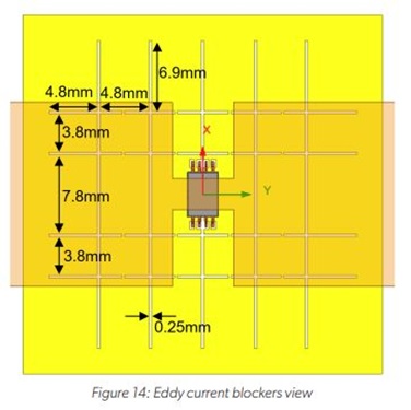
The second option consists in adding some cuts, or eddy current blockers, to the GND plane to prevent any chance for the eddy currents to be induced (Figure 14). In this case, the eddy currents distribution given in Figure 10 helps to find the main current paths.
Ground Plane Hole Below ACS37610
A square hole is considered in the GND plane, below the ACS37610. This square hole has a size HL in both directions. The AC performances are evaluated versus the size of the hole. The results are summarized in Figure 13, with a 10 kHz primary input current.
The main outcome is that the size of the hole should be greater than 20 mm to achieve the same performances as without a GND plane. This is valid for both front and back GND configurations. This is also true for any typical busbar width (W ≤ 30 mm) and any reasonable notch width (N ≤ 10 mm).
Note that the hole can also be a rectangle (with the smallest side greater than 20 mm) or a circle (with a radius greater than 10 mm).
Eddy Current Blockers
The second option consists in cutting the eddy current paths in the ground plane. The main advantage is that the ground plane is mostly preserved. An eddy current blocker is proposed in Figure 14 for the Allegro reference busbar with notch.
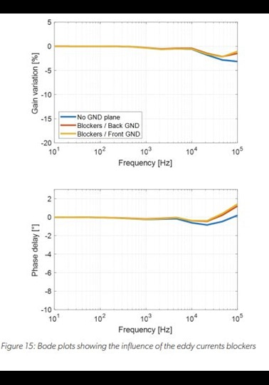
The corresponding AC performances are summarized in Figure 15. The eddy currents in the ground plane are almost fully eliminated, the AC behavior is close to the behavior without the ground plane, and the frequency response is almost flat up to 10 kHz.
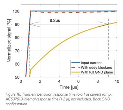
The transient behavior is illustrated in Figure 16. With a 1 µs ramp primary current driven in the busbar, the 90% response time is <0.1 µs with the eddy currents blockers. This is equal to the response time without a ground plane. Again, these results do not include the response time of the ACS37610 itself (<2 µs).
For another combination of busbar and notch, the pattern of eddy blockers might need to be updated. Contact an Allegro representative for any support in this matter.
Conclusions
The PCB ground plane plays a key role in AC and transient performances of a current measurement system based on the ACS37610. A full ground plane right below the ACS37610 will significantly degrade the measurement accuracy of AC current and response time to transient current.
To completely remove these issues, it is recommended to either remove the ground plane below the ACS37610 with at least a 10 mm radius or to cut the eddy currents paths with some smartly positioned trenches in the ground plane.
Contact an Allegro representative for any further questions or support.
Copyright 2023, Allegro MicroSystems. The information contained in this document does not constitute any representation, warranty, assurance, guaranty, or inducement by Allegro to the customer with respect to the subject matter of this document. The information being provided does not guarantee that a process based on this information will be reliable, or that Allegro has explored all of the possible failure modes. It is the customer’s responsibility to do sufficient qualification testing of the final product to ensure that it is reliable and meets all design requirements. Copies of this document are considered uncontrolled documents.