Solving the Challenges of Increasing Power Density by Reducing Number of Power Rails

The world continues to become increasingly electrified, and both the demand for energy and the requirements placed on that energy continue to expand. Between automobile electrification, internet traffic, and renewable energy, a global need has developed for high-power-density technologies that can deliver more power output from the same or less amount of space as legacy solutions. In electrical vehicles, particularly in on-board charger applications, higher power density equates to a smaller, lighter-weight form factor that allows faster charging and frees more space for the battery. This ultimately leads to more driving distance per charge. In data centers, government regulations are driving the need to improve power density. For example, beginning in 2023, the power supply of a European data center must achieve a Titanium Plus efficiency rating (greater than 96 percent efficiency), which effectively doubles power density requirements compared to legacy systems. In microinverters for solar panels, the market continues to push for smaller system size with an increase in power level. This article overviews some of the challenges associated with high-power-density solutions and some of the technologies that can best enable the desired outcome. An innovative technology is then presented that simplifies power-system design for all these markets, with cascading benefits.
Overview of Power Transistor Choices
Common applications today demand high-density power conversion in high-current, high-temperature, high-voltage environments. Achieving the market demand necessitates use of technologies that can support higher switching frequency with reduced conduction losses at much higher temperatures than conventional silicon insulated-gate bipolar transistors (IGBTs) and silicon MOSFETs. The latest trend that allows engineers to achieve the goal of increasing power output while reducing solution size is the adoption of wide-bandgap semiconductors. Wide-bandgap devices—such as silicon carbide (SiC) and gallium nitride (GaN)—have better on-state resistance per specific area than conventional silicon IGBTs and silicon MOSFETs. This performance improvement allows a wide-bandgap power device to enable high-frequency operation and leads to system size reduction.
As described in “Why gate drivers are key to successful electric vehicle designs,” Power Electronics Europe, 2022, Issue 4, for applications that require voltages up to 1700 V, the required high-voltage, high-current, high-temperature performance is better achieved by SiC transistors than silicon IGBTs. Many common applications also demand a small system design with switching speed as fast as 2 MHz. This reduced-size, high-speed switching performance is better served by GaN devices.
Regardless of semiconductor selection—GaN or SiC—achieving the desired performance often requires use of many power devices that must adhere to the strict safety standards established for electric vehicles and various industrial and data-center applications. Meeting these standards requires careful selection of system components. One of the most critical components among these devices is the isolated gate driver, which is used to turn on and turn off the selected transistor.
Understanding the Importance of Gate Drivers and Switch-Matching
The success of a power conversion system is heavily influenced by the isolated gate driver. Isolated gate drivers enable the transfer of data and power between the high-voltage and low-voltage domains, while providing system and human protection from hazardous direct current. Each gate driver must provide a specific control voltage for each of the power switches within the design. The voltage needed for one switch typically differs from the voltage needed for another. Because device switching speed and output quality greatly affect the power conversion, matching the requirements of the switches to the gate drivers is crucial to achieving the desired system performance.
Before selecting a gate driver, the cost, size, weight, reliability, and efficiency of the power-conversion system must be weighed with consideration for the influencing factors, including the environmental conditions presented at the location where the gate driver is placed, component count, and design complexity. The wide variety of conditions that a gate driver will face heavily influence performance. These conditions vary depending on where the gate driver is located—on the high-voltage side of a bridge, on the low-voltage side of a bridge, in the hostile environment of an inverter, or in a charger. In power-conversion circuitry, component count and design complexity also heavily influence device performance. Larger designs result in longer signal paths, which adds parasitics, so smaller gate drives can improve performance. Also, because every component is a potential point of failure, gate drives with reduced component count can improve reliability.
With the vast selection of gate drivers available on the market today, designers have a plethora of options. However, the choice of gate driver is only a starting point. In many applications, it can be challenging to identify a suitable source of power to enable the gate driver to drive the gates of the switches at the required speeds, as discussed next. To meet requirements, power-conversion designs often include multiple bias power supplies that are isolated from the control ground. For a solution that includes multiple tradeoffs in performance, the design challenges that arise from these architectures can consume a significant amount of valuable engineering time, which makes it critical to choose the right gate driver technology early in the design process: The right gate driver can have a big impact on the success of a system.
Understanding the Tradeoffs of Power Rails, Auxiliary Supplies, and Bootstrap Circuitry
In conventional designs, external DC-DC bias supplies are used to drive the gates of the power transistors. Sometimes, application requirements can force the addition of eight or nine separate bias supplies, with each supply adding transformers and other bulky components that degrade reliability and increase solution size. Although the load and stress added by these components can be minimized by design, including these components hinders reliability because every component is a potential point of failure. The added bias supplies not only bring new points of potential for failure, but they must also be sized for the highest operational switching frequency, which results in less-efficient operation at lower frequencies. All things considered, the many complex components and circuitries used in conventional designs add to system cost, size, and weight and reduce reliability.
The task of adding an extra power rail to a design is often more complicated than it first seems. Use of any power supply adds stray capacitance between the control ground and the source terminal of the semiconductor power switch that the gate driver is controlling. For a switch located in the high side of a full bridge, the additional stray capacitance is likely to create common-mode and electromagnetic interference, which brings new design challenges. Also, stray capacitance can allow for the flow of high-voltage current spikes, which can interfere with correct functional operation. These issues are likely to occur even if the power device is driven across an isolation barrier or if the extra power rail is derived from an additional winding on the main system transformer. Furthermore, using an additional winding complicates the design of the main system transformer and can have negative implications when it comes to safety compliance.
A lower-cost alternative method of providing an additional power rail to serve as the external bias supply for the isolated gate driver is to use bootstrap circuitry. The essential components of the bootstrap circuit are a diode, a capacitor, and—in some cases—a resistor. A bootstrap circuit is arranged so that, when the low-side switch is turned on, the capacitor is charged via the diode almost to the level of the supply voltage (Vdd). The capacitor subsequently provides the drive power for the high-side switch. Although this process may seem straightforward, it brings a fresh set of challenges. The diode requires a reverse voltage rating that is higher than the high-voltage bus. In designs with high-frequency switching, this diode must also be rated for fast recovery. The capacitor must be small enough to recharge quickly, but large enough to supply the required gate charge for the switch without becoming discharged too quickly. The resistor, if required, must limit the spikes of charging current flowing into the bootstrap capacitor. This is because all bootstrap designs have the potential for false overcurrent tripping, which would occur if the charging current in the low-side current sense signal to the controller were to spike with sufficient amplitude at the capacitor. To prevent false overcurrent tripping, the amplitudes of such potential spikes must be limited. For that purpose, a resistor is often added in series with the diode. This resistor comes with difficult tradeoffs. Increasing resistor values requires a larger capacitor, which takes more time to charge at startup and thereby delays the availability of high-side drives; yet, if the capacitor is too small, supplying the required gate charge to the high-side switch will come with too much droop in the gate voltage. Together, these requirements typically result in a need that can only be filled by large and relatively expensive components.
Considering the tradeoffs, there is no such thing as an ideal bootstrap circuit. At best, a bootstrap circuit provides a workable tradeoff between multiple design variables. Although this workaround has often been accepted as a required means to an end, it does not satisfy today’s top-notch power-conversion requirements.
The ideal solution for the electrification needs of today might lie in finding a way to eliminate the need for bootstrap circuits and separate power supplies. However, most industry resources have not been devoted to research and development of gate drive systems but rather to wide-bandgap power switches. Driving these switches requires gate drive systems that can fully leverage the potential advantages of these new technologies, including the tremendous benefits that come with the elimination of bootstrap circuits and separate power supplies.
New Approach - Embedding the Bias Supply System Within the Driver
A new approach to driving wide-bandgap power switches is to simplify the way the power switches are driven. Some devices now embed the bias supply system within the driver. These devices need no external auxiliary supply as the bias supply system replaces the need for the external auxiliary supply, eliminating the additional components and design resources associated with auxiliary supplies. In one such approach, the Power-Thru technology from Allegro MicroSystems, power is transferred to the gate drivers using a fully integrated system-in-package (SiP) gate drive (see Figure 1).
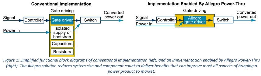
The key subcomponents of the Power-Thru technology are two gate drive ICs and a tiny magnetic-based isolation structure that enables efficient power transfer across the boundary from the low-voltage signal to the high-voltage system. At first, this may seem like an ordinary solution. Compared to the wide range of isolated gate drive ICs on the market, the real and significant novelty is located inside the IC: The Power-Thru technology includes a clever and patented circuit design that allows the IC to manage both the gate drive signal and the transfer of energy from the primary IC to the secondary gate driver IC across the magnetic isolation barrier. This novel technology enables the isolation boundary to carry the drive power required to drive both the external FET switch and the gate drive signal data. Because complete electrical isolation is provided by the magnetic coupling, Power-Thru drivers are equally suitable for use in high-side, low-side, and isolated applications.
The Power-Thru devices remove the need for a bootstrap circuit or an external isolated DC-DC source to create the floating voltage required for controlling the high-side switches. The benefits cascade from there. By eliminating the need to provide an external bias power supply, all the tradeoffs and complexity in choosing the optimal combination of components vanish. The reduced component count/complexity amounts to fewer potential points of failure, which delivers greater reliability, leading to fewer potential warranty claims and enhanced product reputation. The reduced component count also results in smaller gate driver assemblies with shorter signal paths. The shorter signal path inherently results in reduced parasitic capacitance and inductance. As a result, the risk of damage caused by ringing and voltage spikes is significantly reduced and more space is available for the power stages, enabling the use of more-efficient designs. This solution also allows the gate driver to track the power consumption of the gate control with the switching frequency, enabling automatic optimization of efficiency.
By enabling the elimination of auxiliary power supplies, Power-Thru gate drivers ultimately make design and qualification easier while lessening strain on engineering resources and accelerating research and development cycles.
Simplifying Power-Conversion Design by Applying Power-Thru Solutions
Cost, design time, and unexpected problems: These are three of the most significant issues on the minds of project managers who are involved with the design of power conversion systems, and the innovative Power-Thru technology from Allegro can help to minimize all of them. The following example of an on-board charger illustrates the significant impact of the Power-Thru technology.
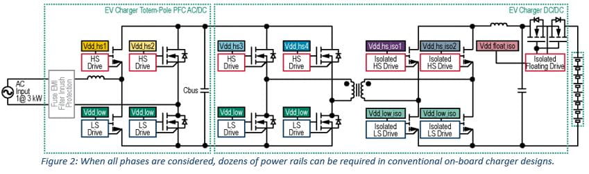
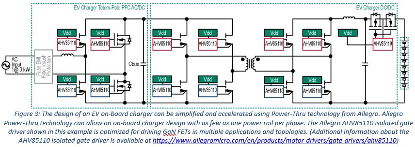
This example uses a multilevel topology, which is known to enable high-efficiency power conversion. However, the design of a multilevel topology is very complex—particularly the gate driver. Each wide-bandgap power transistor of the on-board charger used in this example requires one gate driver to switch the power device. While the primary and secondary low-side switches share the respective power rail, each of the seven high-side switches requires its own isolated bias supply. This can result in nine separate bias rails for the system, which is extremely complex, as shown in Figure 2. When designing the same on-board charger with isolated gate drivers enabled by the Allegro Power-Thru technology, the nine power rails per phase can be merged into a single rail, as illustrated in Figure 3. This break-through system design and build simplification allows significantly reduced component count. All power stages can be implemented in a single board, only requiring a single capacitor and two resistors on the output, which speeds design time and improves the likelihood of early design success. Furthermore, the reduced component count reduces bill of material (BOM) costs and system size, and also unlocks new levels of build simplification.
By reducing complexity, early success in testing and validation is more likely, and application of the technology can be more reliable because use of fewer parts equates to less opportunity for a failure. More importantly, the reduction of system size enables an increase in power density as the same amount of power can be delivered with smaller form factor.
Unlocking New Levels of Conversion Performance and Simplification with Power-Thru
In summary, power conversion systems need to be ever more efficient, compact, reliable and, ideally, less expensive. Wide-bandgap power switches allow for significant advances in achieving higher efficiency and higher power density, but they add system complexity and cost. Reducing system complexity can be achieved by focusing on another critical part of the power conversion system—the driving of the power FETs. The approach used to drive a power switch can have great impact on the solution as a whole, and drivers that enable the elimination of multiple power rails and bootstrap circuits have cascading benefits to the system.
The new paradigm in power conversion—created by the Power-Thru technology inside Allegro high-voltage isolated gate drivers—uses a novel SiP gate drive that includes a magnetic coupling device placed in between the primary and secondary gate driver integrated circuits, which eliminates the need for bias supplies. The power needed to drive the gate of the switch is transferred with the gate on/off logic signals, thus completely eliminating the external auxiliary power required by conventional solutions. The Power-Thru technology enables shorter signal paths that reduce parasitics and voltage spikes, increase reliability, free up space, and lead to more-efficient designs. The embedded bias eliminates bootstrap circuitry, separate power supplies, and other complicated design tradeoffs.
Considered as whole, the Power-thru technology provides advantages in all relevant system dimensions, unlocking significant system and design simplification, higher efficiency, and reduced component count leading to higher power density and reliability.
Based on the article, "Solving the Challenges of Increasing Power Density By Reducing Number of Power Rails" by Andy Wang, originally published in Power Electronics Europe. Republished with permission. For portions not copyrighted by original publisher, Copyright ©2023, Allegro MicroSystems, Inc.
The information contained in this document does not constitute any representation, warranty, assurance, guaranty, or inducement by Allegro to the customer with respect to the subject matter of this document. The information being provided does not guarantee that a process based on this information will be reliable, or that Allegro has explored all of the possible failure modes. It is the customer's responsibility to do sufficient qualification testing of the final product to ensure that it is reliable and meets all design requirements. Copies of this document are considered uncontrolled documents.