Unipolar Hall-Effect Sensor IC Basics
There are four general categories of Hall-effect IC devices that provide a digital output: unipolar switches, bipolar switches, omnipolar switches, and latches. Unipolar switches are described in this application note. Similar application notes on bipolar switches, omnipolar switches, and latches are provided on the Allegro website.
Unipolar Hall-effect sensor ICs, often referred to as "unipolar switches," are operated by a positive magnetic field. A single magnet presenting a south polarity (positive) magnetic field of sufficient strength (magnetic flux density) will cause the device to switch to its on state. After it has been turned-on, the unipolar IC will remain turned-on until the magnetic field is removed and the IC reverts to its off state.
An application for detecting the position of a vehicle gear-shift lever is shown in figure 1. The gear-shift lever incorporates a magnet (the red-and-blue cylinder). The line of miniature black boxes is an array of unipolar switch devices. When the vehicle operator moves the lever, the magnet is moved past the individual Hall devices. The devices near the magnet are subjected to the magnetic field and are turned-on, but more remote devices are not affected and remain turned-off. Note that the south pole of the magnet (colored red) is toward the Hall devices, and that the Hall devices are oriented with the branded face of the device toward the magnet south pole.
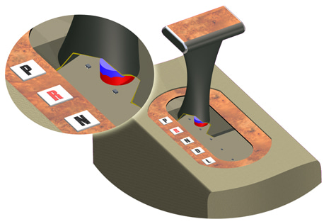
Figure 1. An application using unipolar switch sensor ICs. The ultra-small Hall ICs switch as the magnet (red and blue cylinder) moves past them during gear-shifting.
Magnetic Switchpoint Terms
The following are terms used to define the transition points, or switchpoints, of Hall switch operation:
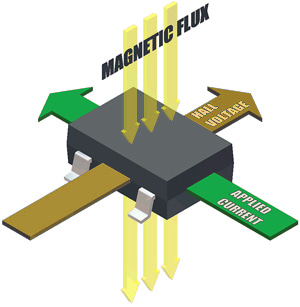
Figure 2. The Hall effect refers to the measurable voltage present when an applied current is influenced by a perpendicular magnetic field.
- B − The symbol for Magnetic Flux Density, the property of a magnetic field used to determine Hall device switchpoints. Measured in gauss (G) or tesla (T). The conversion is 1 G = 0.1 mT.
B can have a north or south polarity, so it is useful to keep in mind the algebraic convention, by which B is indicated as a negative value for north-polarity magnetic fields, and as a positive value for south-polarity magnetic fields. This convention allows arithmetic comparison of north and south polarity values, where the relative strength of the field is indicated by the absolute value of B, and the sign indicates the polarity of the field. For example, a − 100 G (north) field and a 100 G (south) field have equivalent strength, but opposite polarity. In the same way, a − 100 G field is stronger than a − 50 G field.
- BOP − Magnetic operate point; the level of a strengthening magnetic field at which a Hall device switches on. The resulting state of the device output depends on the individual device electronic design.
- BRP − Magnetic release point; the level of a weakening magnetic field at which a Hall device switches off (or for some types of Hall devices, the level of a strengthening negative field given a positive BOP). The resulting state of the device output depends on the individual device electronic design.
- BHYS − Magnetic switchpoint hysteresis. The transfer function of a Hall device is designed with this offset between the switchpoints to filter out small fluctuations in the magnetic field that can result from mechanical vibration or electromagnetic noise in the application. BHYS = | BOP − BRP |.
Typical Operation
When a unipolar switch turns on, the resulting output signal can be either at logic high or logic low, depending on the design of the device IC output stage. Figure 3 shows the possible output states of unipolar switches. The top panel represents a switch designed to output logic low (at the output transistor saturation voltage, VOUT(sat), usually <200 mV) in a strong south polarity field. The bottom panel represents a switch designed to output logic high (up to full supply voltage, VCC) under the same conditions.
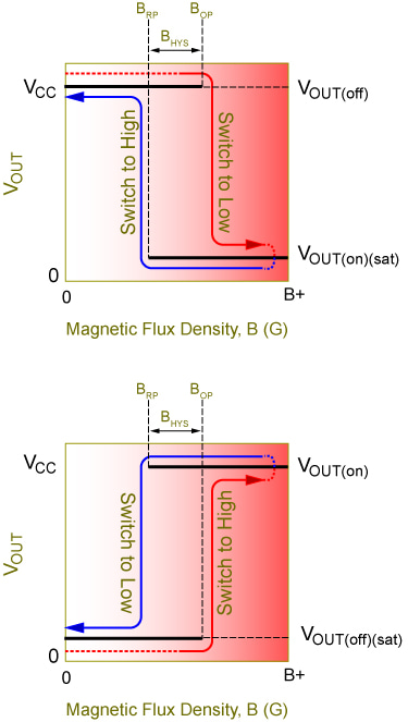
Figure 3. Unipolar switch output characteristics. The top panel displays switching to logic low in the presence of a strong south polarity field, and the bottom panel displays switching to logic high, also in a south polarity field.
Although the device could power-on with the magnetic flux density at any level, for purposes of explanation of figure 3, start at the far left, where the magnetic flux (B, on the horizontal axis) is less positive than BRP or BOP. Here the device is off, and the output voltage (VOUT, on the vertical axis) depends on the device design: high (top panel), or low (bottom panel).
Following the arrows toward the right, the magnetic field becomes increasingly positive. When the field is more positive than BOP, the device turns on. This causes the output voltage to change to the opposite state (either to high or to low, depending on the device design).
While the magnetic field remains more positive than BRP, the device remains turned-on, and the output state remains unchanged. This is true even if B becomes slightly less positive than BOP, within the built-in zone of switching hysteresis, BHYS.
Following the arrows back toward the left, the magnetic field becomes less positive. When the magnetic field again drops below BRP, the device turns off. This causes the output to change back to the original state.
Pull-Up Resistor
A pull-up resistor must be connected between the device supply and the output pin (see figure 4). Common values for pull-up resistors range from 1 to 10 kΩ. The minimum pull-up resistance is a function of the Hall IC maximum output current (the devices usually are designed to sink current) and the supply voltage. 20 mA is a typical maximum output current, and in that case the minimum pull-up would be VCC / 0.020 A.
In applications where current consumption is a concern, the pull-up resistance could be as large as 50 to 100 kΩ. Caution however is required because large pull-up values make it possible to induce external leakage currents to ground. This is not a device problem, rather the leakage occurs in the conductors between the pull-up resistor and the device output pin. These currents could be high enough to reduce the output voltage, regardless of the state of the magnetic field and device switching state. Taken to the extreme, this can reduce the output voltage enough to inhibit proper external logic functions.
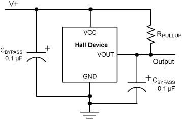
Figure 4. Typical application diagram.
Use of Bypass Capacitors
Refer to figure 4 for a layout of bypass capacitors. In general:
- For designs without chopper stabilization − It is recommended that a 0.01 µF capacitor be placed between the output and ground pins and between the supply and ground pins.
- For designs with chopper stabilization − A 0.1 µF capacitor must be placed between the supply and ground pins, and a 0.01 µF capacitor is recommended between the output and ground pins.
Power-On Time
Power-on time depends to some extent on the device design. Digital output devices, such as the unipolar switch, reach stability with the following approximate delays:
| Device type | Power-on time |
| Without chopper-stabilization | <1 µs |
| With chopper-stabilization | <25 µs |
Basically, this means that prior to this elapsed time after providing power, device output may not be in the correct state, but after this time has elapsed, device output is guaranteed to be in the correct state.
Power Dissipation
Total power dissipation is the sum of two factors:
- Power consumed by the Hall device, excluding power dissipated in the output. This value is VCC times the supply current. VCC is the device supply voltage and the supply current is usually specified on the datasheet. For example, given VCC = 12 V and supply current = 9 mA, power dissipation = 12 × 0.009 or 108 mW.
- Power consumed in the output transistor. This value is V(sat) times the output current (set by the pull-up resistor). If V(sat) is 0.4 V (worst case) and the output current is 20 mA (often worst case), the power dissipated is 0.4 × 0.02 = 8 mW. As you can see, because of the very low saturation voltage the power dissipated in the output is not a huge concern.
Total power dissipation for this example is 108 + 8 = 116 mW. Take this number to the derating chart in the datasheet for the package in question and check to see if the maximum allowable operational temperature must be reduced.
Frequently Asked Questions
Q: How do I orient the magnet relative to the Hall device?
A: The magnet south pole is directed towards the branded face of the device package. The branded face is where you will find the identification markings of the device, such as partial part number or date code.
Q: How does a north polarity, or negative, magnetic field affect a unipolar switch?
A: A north polarity, or negative, field has no effect on a unipolar switch.
Q: Can I approach the device package back side with the magnet?
A: Yes, however bear this in mind: if the poles of the magnet remain oriented in the same direction, then the orientation of the flux field through the device remains unchanged from the front-side approach (for example, if the south pole was nearer the device in the front-side approach, then the north pole would be nearer the device in the back-side approach). The north pole would then generate a positive field relative to the Hall element, while the south pole would generate a negative field.
Q: Are there trade-offs to approaching the device back side?
A: Yes. A "cleaner" signal is available when approaching from the package front side, because the Hall element is located closer to the front side (the package branded face) than to the back side. For example, for the "UA" package, the chip with the Hall element is 0.50 mm inside the branded face of the package, and so approximately 1.02 mm from the back-side face. (The distance from the branded face to the Hall element is referred to as the "active area depth.")
Q: Can a very strong magnetic field damage a Hall-effect device?
A: No. A very strong field will not damage an Allegro Hall-effect device nor will such a field add additional switchpoint hysteresis (other than the designed hysteresis).
Q: Why would I want a chopper-stabilized device?
A: Chopper-stabilized sensor ICs allow greater sensitivity with more-tightly controlled switchpoints than non-chopped designs. This may also allow higher operational temperatures. Most new device designs utilize a chopped Hall element.
Suggested Devices
Allegro unipolar devices are listed in the selection guides on the company website, at Switches and Latches.
Applications
- Vane interrupter switching
- Proximity sensing
- Seat position sensing
- Seat belt buckle sensing
- Open/close door or lid sensing
- Pulse counter
- Cell phone flip switch
- Speed sensing
Application Notes on Related Device Types
Reference: AN296069