DCDC Regulators
Low Input Voltage, Dual Synchronous Buck Regulator with Synchronization and Independent Enables
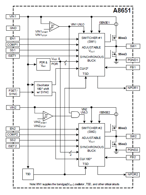
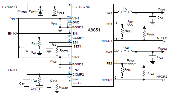
A8651
The A8651 offers efficient and flexible power conversion for low-voltage applications, featuring dual 2A synchronous buck regulators with adjustable output voltage, synchronizable switching frequency, and independent enable/NPOR outputs.
Product Details
Product Details
Top Features
- AEC-Q100 Qualified
- Operating voltage range: 2.5 to 5.5 V
- UVLO stop threshold: 2.25 V (max)
- Dual outputs with up to 2 A output current per regulator
- Adjustable output voltage as low as 0.8 V
- Internal 80 mΩ high-side switching MOSFET
- Internal 55 mΩ low-side switching MOSFET
- Adjustable switching frequency ( fSW ): 0.35 to 2.2 MHz
- Synchronizes to external clock: 1.2 × to 1.5 × fOSC
- 180° phase shift between switching regulators
- Sleep mode supply current less than 5 μA
- Soft start time externally set via the SS pin
- Pre-biased startup capable
- Externally adjustable compensation
- Stable with ceramic output capacitors
- Independent enable inputs and NPOR output pins
- NPOR delay of 7.5 ms (A8651) or 120 μs (A8651-1)
- Adjustable current limiting (OCP) for each regulator
- Hiccup mode short-circuit protection (HIC)
- Overvoltage and overtemperature protection
- Open-circuit and adjacent pin short-circuit tolerant
- Short-to-ground tolerant at every pin