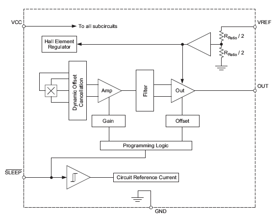
Micropower 3 V Linear Hall-Effect Sensor ICs with Tri-State Output and User-Selectable Sleep Mode

A1391, A1392, A1393, A1395

A1391-2 Product Image

Description

Top Features

Packaging

The A139x family of linear Hall-effect sensor integrated circuits (ICs) includes the A1391, A1392, A1393, and the A1395 products. The entire A139x family provides a voltage output that is directly proportional to an applied magnetic field. Before amplification, the sensitivity of typical Hall effect ICs (measured in mV/G) is directly proportional to the current flowing through the Hall effect transducer element inside the ICs. In many applications, it is difficult to achieve sufficient sensitivity levels with a Hall effect sensor IC without consuming more than 3 mA of current. The A139x minimize current consumption to less than 25 µA through the addition of a user-selectable sleep mode. This makes these devices perfect for battery-operated applications such as: cellular phones, digital cameras, and portable tools. End users can control the current consumption of the A139x by applying a logic level signal to the SLEEP pin. The outputs of the devices are not valid (high-impedance mode) during sleep mode. The high-impedance output feature allows the connection of multiple A139x Hall effect devices to a single A-to-D converter input.

The quiescent output voltage of these devices is 50% nominal of the ratiometric supply reference voltage applied to the VREF pin of the device. The output voltage of the device is not ratiometric with respect to the SUPPLY pin.

Despite the low power consumption of the circuitry in the A139x, the features required to produce a highly-accurate linear Hall effect IC have not been compromised. Each BiCMOS monolithic circuit integrates a Hall element, improved temperature-compensating circuitry to reduce the intrinsic sensitivity drift of the Hall element, a small-signal high-gain amplifier, and proprietary dynamic offset cancellation circuits. End of line, post-packaging, factory programming allows precise control of device sensitivity and offset.

  • High-impedance output during sleep mode
  • Compatible with 2.5 to 3.5 V power supplies
  • 10 mW power consumption in the active mode
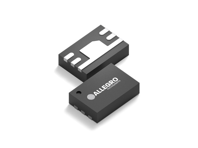
  • Miniature MLP package
  • Ratiometric output scales with the ratiometric supply reference voltage (VREF pin)
  • Temperature-stable quiescent output voltage and sensitivity
  • Wide ambient temperature range: –20°C to 85°C
  • ESD protection greater than 3 kV
  • Solid-state reliability
  • Preset sensitivity and offset at final test

These devices are available in a small 2.0 × 3.0 mm, 0.75 mm nominal height microleaded package (MLP/DFN), suffix EH. It is Pb (lead) free, with 100% matte tin leadframe plating.

EH Package Documentation

Part Number Specifications and Availability

Documentation and Resources

Documentation

Filter Document Type:
All Types
All Types Application Note
Documents Found: 32