
Deconstructing Current Sensor Accuracy: Understanding Dynamic and Environmental Errors
Introduction
The accuracy of a linear current sensor is built on a simple foundation. Every linear device implements the ideal transfer function, in which the output voltage is a straight-line function of the primary current. Two parameters define that line: the sensitivity (Sens), which is its slope; and the quiescent voltage output (VQVO), which is its zero-current intercept.
Correspondingly, the two most fundamental accuracy terms are sensitivity error, a deviation in the slope that is proportional with the measured current and therefore dominates at the high end of the range, and offset (or QVO) error, a constant intercept deviation that is independent of current and dominates at low currents. These two parameters describe the baseline behavior of the sensor.
The previous installment of this series, Current Sensor Accuracy Fundamentals: Understanding Sensitivity and Offset Error, established these two foundational pillars upon which all current sensor accuracy rests.
In a real electric vehicle (EV) traction inverter, an onboard charger, a solar string inverter, or an industrial motor drive, the sensor is continuously subjected to wide temperature swings, fluctuating supply rails, high-frequency switching noise from silicon carbide (SiC) and gallium nitride (GaN) power stages, mechanical stress from potting and vibration, stray magnetic fields radiated by adjacent conductors, and lifetime aging. These influences do not introduce a fundamentally new kind of error. Instead, each influence ultimately manifests as a disturbance of the same two parameters introduced in the previous document in this series: Every environmental and dynamic factor shifts either the slope (sensitivity) or the intercept (offset) of the transfer function. The central task of real-world accuracy engineering, therefore, is not to memorize a long list of unrelated error sources but to understand how much each operating condition disturbs these two underlying parameters.
This document deconstructs many error sources, beyond the baseline sensitivity and offset terms, that are relevant to both field-based (coreless and core-based) and integrated conductor current sensors (Hall-effect, tunneling magnetoresistance [TMR]).
Supply-related errors cover power-supply rejection and ratiometry, i.e., how the sensor responds to an imperfect or fluctuating VDD rail, and how a properly architected ratiometric system can cancel that fluctuation entirely.
Environmental and physical errors address temperature drift, mechanical and package stress, magnetic hysteresis, stray external fields, and nonlinearity, which is the deviation or the bowing of the transfer function that survives even after gain and offset are calibrated.
Dynamic and AC-performance errors examined in this document are bandwidth, phase shift, step response, propagation delay, total output noise, and common-mode transient immunity (CMTI). These parameters govern whether a sensor can both resolve a quiet signal and react quickly enough to protect the power stage during a fault.
Finally, lifetime and aging effects quantify how the foundational parameters drift over the full-service life of the product.
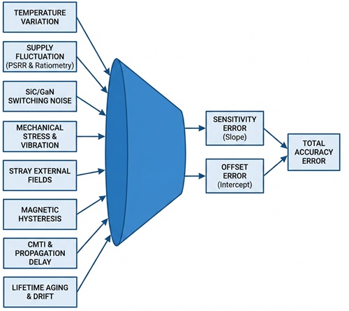
This document demonstrates how to combine all these individual contributions into a single total error figure, distinguishes between the conservative worst-case (linear) summation and statistical root-sum-of-squares (RSS) methods, and directs when to use each method. With this framework, a designer is equipped to move confidently from an advertised accuracy specification to a calculated estimation of real-world in-system performance throughout the specified temperature range and operational life of the product.
Current Sensor Error: The Accuracy Parameters
A review of the previous part of this series is provided here. Every accuracy term presented can be traced back to one of two effects: a change in the slope of the transfer function (sensitivity) or a change in the zero-current intercept of the transfer function (offset). The parameters described below are simply the named, measurable ways those two effects present, whether the place of origination is in the silicon, the magnetic circuit, or the system environment.
Sensitivity Error
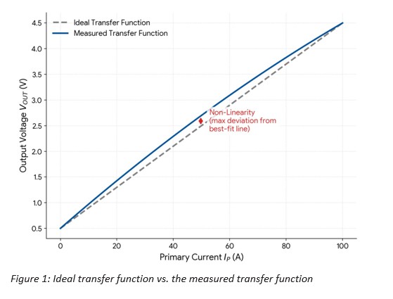
Sensitivity (Sens) is the slope of the transfer function, the change in output voltage per unit of measured primary current, typically expressed in mV/A or mV/G. Sensitivity error is the deviation of the actual slope from its ideal value. When current is near zero, sensitivity error is negligible. However, it grows linearly with current, to its maximum at full scale. Therefore, at the high end of the measurement range, sensitivity error dominates the total error budget.
Physically, sensitivity error arises from tolerances in the magnetic coupling between the primary conductor and the sensing element, as well as gain tolerance in the front-end amplifier and over the operating range. These tolerances result in a slope that drifts as the die heats and cools. Allegro factory-trims sensitivity at production test and applies internal temperature compensation to hold the accuracy of the sensor within a tight band throughout the automotive range. At the system level, residual sensitivity error can be further reduced through the two-point (gain and offset) calibration, in which a known reference current near full scale is used to solve for and correct the true slope.
Offset Error/Quiescent Voltage Offset Error
The quiescent voltage output (VQVO) is the sensor output when zero primary current flows, i.e., the intercept of the transfer function. Offset error (also called quiescent voltage offset error [QVO error]) is the deviation of that intercept from its ideal value. Unlike sensitivity error, offset is a fixed voltage that is independent of the measured current, so it is conventionally expressed as a voltage (mV). Offset error dominates the total error budget at the low end of the measurement range, exactly where resolution is already most challenged by noise.
Offset originates from mismatch in the Hall plate, input-referred offset in the front-end amplifier, stress in the mechanical package, and fluctuations in temperature. Allegro mitigates the static and thermal components using chopper-stabilization and dynamic offset-cancellation techniques together with internal digital temperature compensation. At the system level, offset is the single easiest error to remove: A one-time single-point offset zeroing method, performed with the controller while the system is known to be at zero current, is used to capture VQVO and subtract it from all subsequent readings. Because offset dominates low-current accuracy, this yields the largest accuracy improvement per unit of effort for low-current measurement.
Supply-Related Errors
Every current sensor is ultimately powered by a supply rail, and in application, no rail is perfectly stable. Line and load transients, regulator tolerance, temperature drift of the LDO, and high-frequency ripple coupled from adjacent switching stages all cause VDD to deviate from its nominal value. Because both the quiescent output voltage and the sensitivity of a linear sensor are referenced to that supply, any movement of the rail has the potential to move the transfer function. The two parameters that quantify this behavior are power-supply rejection and ratiometry. Understanding the distinction between them, and how they interact with the downstream analog-to-digital converter (ADC), is the difference between a system that fights supply noise with expensive regulation and one that cancels it architecturally.
Power Supply Rejection
The power supply rejection ratio (PSRR) describes how effectively the internal circuitry of the sensor isolates its output from the variations on the VDD rail that are not intended to scale the output. It is most relevant to nonratiometric (fixed-reference) devices and to the high-frequency behavior of all devices, where ripple from a nearby DC-DC converter or inverter stage can couple onto the supply faster than any ratiometric reference can track. A sensor with high PSRR attenuates this ripple before it reaches the signal chain, and the ripple appears at the output as a small residual offset or gain disturbance. At the board level, PSRR is complemented by good decoupling practice: placement of low-ESR ceramic capacitors immediately adjacent to the VDD and GND pins provides a local charge reservoir that smooths fast transients and shunts high-frequency noise to ground before the noise can modulate the sensor output. Because this residual disturbance manifests as a shift in either offset (dominant at low current) or sensitivity (dominant at high current), it must be carried into the total error budget for any application with a noisy or lightly-regulated rail.
Ratiometry and Ratiometry Error
Ratiometry is a deliberate architectural feature in which both the quiescent output voltage (VQVO) and the sensitivity scale in direct proportion to the supply voltage. In a perfectly ratiometric device, a +3% increase in VDD produces exactly a +3% increase in both the zero-current output and the slope of the transfer function. Viewed at the analog output alone, this looks like an error: The output has moved even though the primary current has not. The insight that makes ratiometry powerful is that this “error” can be canceled at the system level. Because power for the sensor and the reference input (VREF) of the microcontroller ADC is from the same rail, the conversion window of the ADC scales with the sensor output. If VDD increases 3%, the sensor output increases 3% and the ADC full-scale reference increases 3%, so the resulting digital code is unchanged. The supply drift cancels, and the measurement remains stable.
The practical payoff is significant: ratiometry allows designers to meet tight accuracy targets using standard, cost-effective low-dropout oscillators (LDOs) rather than expensive, ultra-high-precision voltage references. Ratiometry error is the specification that quantifies the imperfection in this proportional tracking, the small residual by which the sensor fails to scale exactly with the rail. Unlike the bulk supply variation it corrects, ratiometry error survives the ADC conversion and cannot be canceled by the shared-reference technique. It must therefore be included explicitly in the total error budget. A poor ratiometry specification erodes the benefit of the architecture and should weigh in the device selection for supply-sensitive designs.
Environmental and Physical Factors
For supply-related errors that originate in the electrical domain, there are environmental and physical factors that act on the sensor through the thermal, mechanical, and magnetic domains. Yet, the principle established earlier holds: These influences do not introduce a fundamentally new category of error. Each influence ultimately expresses itself as a shift in the slope (sensitivity) or the intercept (offset) of the transfer function: Temperature shifts both the sensitivity and the offset; mechanical stress predominantly shifts offset; stray fields and hysteresis add contributions that masquerade as real current; and nonlinearity is the residual bowing of the transfer function that survives even after gain and offset are perfectly calibrated.
Temperature Variation/System Operating Environment
Operating temperature is one of the most significant influences on current sensor accuracy, and it is unique in that it disturbs both foundational parameters at once. As the die heats and cools throughout the automotive range of −40°C to 150°C, the gain of the magnetic front end drifts, which shifts sensitivity, while mismatch and thermal effects in the signal chain shift the quiescent output voltage. The offset drift is particularly detrimental at low current levels, where the signal-to-noise ratio is already lowest and offset dominates the error budget. Allegro current sensors counter this offset drift with internal temperature compensation that maintains both sensitivity and offset within a tight band throughout the full temperature range. Because the same physical variable of temperature affects multiple internal contributors, these contributing terms are correlated and should be treated as such in the error budget; they should not be combined by root-sum-of-squares as if they were independent. Beyond the silicon, the designer must also remember that the PCB itself expands and contracts with temperature, which couples thermal effects into the mechanical-stress mechanism described next.
Stress/Vibration/Mechanical
The Hall effect is inherently sensitive to mechanical stress through the piezo-Hall effect, in which strain in the silicon lattice alters the carrier mobility and therefore the response of the sensing element. Pressure exerted by potting compounds, the sustained vibration common in industrial motor drives, and the cyclic expansion and contraction of the PCB during thermal cycling all impose stress on the die and manifest primarily as a shift in the offset voltage. Because this shift is a physical deformation of the sensing element rather than an electrical artifact, it cannot be trimmed away at the factory, it is dependent on how the finished assembly is mounted and packaged. The most effective mitigation is therefore mechanical: The critical factor for maintained long-term accuracy is the design of a housing, mounting-scheme, and potting-geometry that minimizes direct and asymmetric pressure on the sensor package. Allegro stress-compensation techniques reduce the sensitivity of the silicon to these effects, but mechanical design at the system level remains the most important in mitigation of mechanical effects.
Magnetic Hysteresis
Magnetic hysteresis is the “memory” effect of ferromagnetic materials. If a sensor is exposed to a large current surge, like a short-circuit event, a small amount of residual magnetism can remain in any ferromagnetic material near the sensing path, such as a leadframe or a concentrating core. When the current returns to zero, this residual magnetization produces a small but persistent offset shift known as magnetic hysteresis error. Because it appears as a fixed offset, magnetic hysteresis error is most damaging to low-current accuracy; and, because it is triggered by an event rather than a steady operating condition, this condition can persist until the next power cycle or other re-zeroing event.
Stray External Fields
Stray magnetic fields, also called common-mode or external fields, are among the most common real-world corruptors of current measurement. They radiate from nearby current-carrying conductors, busbars, transformers, motors, and other electromagnetic devices; and, because the sensor cannot inherently distinguish a stray field from the field produced by its own primary current, the direct appearance of an uncompensated stray field is that of a false current reading. The primary architectural defense is differential sensing: by placement of two sensing elements and measurement of the difference between them, a uniform external field couples equally into both elements and cancels, while the intended differential signal from the primary conductor survives. Allegro differential current sensors reject common-mode fields and maintain accuracy in electrically noisy environments. When differential rejection alone is insufficient, additional mitigations can be used. First, optimize sensor orientation, placement, and geometry and layout of the current-carrying conductors to minimize coupling. Second, increase the distance between the sensor and the interfering source. Last, add a magnetic shield to redirect or absorb the external field. Shielding is effective but adds cost, size, and its own hysteresis considerations, so it should be reserved for applications where placement and orientation cannot adequately solve the problem.
System Noise (Environmental Coupling)
The electrical environment couples high-frequency switching noise from nearby inverters and DC-DC converters directly into the sensor signal path. While this is not a DC accuracy term in the same sense as offset or sensitivity, it degrades the effective resolution of the measurement and can trip protection thresholds falsely. An external resistor-capacitor (RC) filter on the sensor output is the standard mitigation, but it involves a direct tradeoff with bandwidth and propagation delay.
Dynamic and AC Performance Errors
While DC accuracy parameters like sensitivity and offset define the static performance of a sensor, real-world power electronics are highly dynamic. Traction inverters, onboard chargers, and industrial motor drives switch heavy currents at high frequencies, which demands that the current sensor not only measure the amplitude accurately but also respond fast enough to maintain the stability of control loops and to protect the power stage from catastrophic faults. The parameters that govern this behavior—bandwidth, noise, propagation delay, and common-mode transient immunity (CMTI) —are heavily intertwined. An improvement to one often requires a tradeoff for another. This forces designers to make careful architectural choices in the routing of the sensor output.
Frequency Response and Phase Shift
Every current sensor has a finite bandwidth, ranging from 80 kHz to 10 MHz. As the frequency of the measured primary current approaches this bandwidth limit, the sensor output experiences two effects: the signal magnitude attenuates, and the output signal lags the actual physical current, which creates a phase shift. In a high-speed digital control loop, such as field-oriented control (FOC) in an electric vehicle traction inverter, excessive phase shift consumes the system phase margin. Without careful minimization of, and accommodation for, the phase shift of the sensor, the motor control algorithm can destabilize, which leads to inefficient commutation or oscillations.
Total Output Noise (RMS/Peak-to-Peak)
Noise establishes the resolution floor of a current sensor; it is the smallest current change the device can resolve regard-less of how well offset and gain are calibrated. Sensor noise is fundamentally characterized by its noise density, expressed in nV/Hz (referred to the output) or equivalently in mA/Hz (referred to the measured current).
The total integrated RMS noise at the output is obtained as the noise density multiplied by the square root of the measurement bandwidth. The square-root relationship reveals a physical design tradeoff: resolution fights speed. If an application only needs to resolve slowly-varying currents, a designer can band-limit the sensor output with an external RC filter, which can drastically lower the noise floor and thereby improve low-current resolution. Because low-current accuracy is governed by the combination of offset error and noise, this simple filtering technique is highly effective for precision metering tasks.
For specification and worst-case design, RMS noise is frequently converted to peak-to-peak noise using a crest factor. Assuming gaussian-distributed noise, a 6.6× multiplier captures approximately 99.9% of the noise excursions. Therefore, designers should be careful to compare sensors on the same basis: A part specified in RMS always appears quieter than the same part specified peak-to-peak. In practical terms, if an application measures a 100 A signal with a sensor whose output noise corresponds to 50 mA RMS, the resolvable signal-to-noise ratio is excellent at full scale but degrades proportionally at near-zero current.
Step Response and Propagation Delay
Like frequency response and phase shift describe the sensor behavior in the frequency domain, step response and propagation delay describe the same dynamics in the time domain and are the most-important parameters for fault protection. Propagation delay is the time between a change in the primary current and the appearance of the corresponding change at the sensor output, measured at a defined threshold (commonly 20% of the input and output points).
Response time or rise time is the time required for the output to slew from 10% to 90% of its final value following a current step. In an overcurrent or short-circuit event, the total time available to detect the fault and command the power stage to shut down is the sum of the sensor propagation delay, the comparator/ADC latency, and the gate-driver turn-off time. With fast-switching SiC and GaN power stages capable of catastrophic failure within microseconds, the minimization of sensor propagation delay becomes exceedingly important.
The tradeoff between the noise-reduction benefit of band-limiting, as discussed above, and the speed requirement of fast fault detection is inherent: Every pole added to the signal chain to reduce noise also slows the step response and increases the propagation delay. A robust design therefore separates the two concerns—often with a fast, wide-bandwidth path tapped for the overcurrent comparator and a slower, filtered path fed to the measurement ADC. Allegro current sensors are characterized for both propagation delay and response time so that designers can budget total fault-response latency with confidence rather than estimating it from bandwidth alone.
Common-Mode Transient Immunity (CMTI)
In modern traction inverters and on-board chargers, the transition to SiC and GaN power stages introduces unprecedented slew rates, often in excess of 100 kV/μs. These extreme voltage transients (dV/dt) present a severe challenge for current measurement: Capacitive coupling between the high-voltage primary conductor and the low-voltage sensor signal chain can inject massive common-mode noise that leads to a falsely tripped fault or corrupted ADC readings.
Common-mode transient immunity (CMTI) quantifies the ability of a sensor to reject these high-speed voltage spikes and maintain a stable output simultaneously. Integrated-conductor sensors, particularly those with differential Hall-effect or TMR sensing elements, inherently reject common-mode magnetic interference; however, they must also employ advanced electrostatic shielding and internal layout isolation to achieve high CMTI. To preserve the inherent CMTI performance of the sensor during violent switching events, the PCB design must minimize the parasitic overlap capacitance between the switch-node copper pours and the analog output traces of the sensor.
Improving Accuracy: Calibration Techniques
Because the errors collapse onto just two parameters, a small number of well-chosen in-application measurements can correct most of the real-world error of the system. Even the best factory-trimmed sensor benefits from in-application calibration: The factory can only trim the silicon, it cannot know the DC bias of the surrounding system, the mechanical stress imposed by the final assembly, or the exact gain of the downstream signal chain. The techniques below increase in capability and cost.
Single-Point Offset Zeroing
The simplest and highest-value calibration is single-point off-set zeroing. While the system is known to be at zero primary current, for example, during a controlled idle state at power-up, the controller samples the sensor output and stores that reading as the true zero reference and subtracts the value it from all subsequent measurements. In a single inexpensive step, this removes not only the offset (QVO) error of the sensor itself, but also any system-level DC bias contributed by the downstream amplifier, ADC, or board-level effects. Because offset error dominates the total error budget at low currents, where the signal-to-noise ratio is already most challenged, single-point zeroing delivers the largest accuracy improvement per unit of effort of the techniques available. It corrects the intercept of the transfer function but leaves the slope untouched, so it is the ideal choice when low-current accuracy is the priority and full-scale gain accuracy is already adequate.
Two-Point (Gain and Offset) Calibration
When both low and high-current accuracy matter, two-point calibration is the appropriate next step. Here the output is measured at two known currents, typically zero and a precisely-known reference current near full scale. With two measured points, the controller can solve simultaneously for the actual slope (sensitivity) and the actual intercept (offset), and it can thereby correct both foundational error terms at once. This technique directly references the two dominant contributors at opposite ends of the range: offset at the low end and sensitivity error at the high end. Its practical requirement is access to a trusted reference current during manufacturing test or periodic field calibration; the accuracy of the correction can never exceed the accuracy of that reference. Two-point calibration corrects the straight-line portion of the transfer function completely.
Choosing the Right Technique
Single-point zeroing corrects offset only, at negligible cost, and should be considered the default for virtually every system. Two-point calibration adds sensitivity correction for modest additional effort and is the mainstay solution for applications that must be accurate at both ends of the range. Critically, calibration cannot remove all noise, temperature-driven drift that occurs after calibration, or event-driven shifts such as magnetic hysteresis. Calibration corrects the deterministic, repeatable portion of the error, while the remaining random and drift terms continue to contribute to the total error budget. The most robust designs combine a one-time factory calibration or end-of-line calibration with a periodic in-system offset re-zeroing method designed to identify slow drift over the life of the product.
Lifetime Accuracy
Every accuracy number discussed so far describes the sensor at a single moment in time, typically fresh out of the box, at room temperature, on a test bench. However, a current sensor in an EV traction inverter, a solar string inverter, or an industrial drive must hold its accuracy not for a moment but for a service life measured in years and tens of thousands of operating hours. Lifetime accuracy is a discipline that quantifies how the two foundational parameters drift over that full-service life and guarantees that, even in the worst case, the total error remains within the safety and performance limits of the system. Just as with every other error family described here, aging does not introduce a fundamentally new kind of error; it simply causes slow, additional shifts in slope and intercept that must be budgeted from day one rather than discovered in the field.
Lifetime Error
Lifetime accuracy is the worst-case error expected over the entire operational life of the sensor. It combines the initial error with the additional drift accumulated through thousands of hours of thermal, electrical, and mechanical stress. The correct practice is to design the error budget based on the lifetime figure.
Drift Mechanisms
Lifetime drift arises from the slow physical evolution of the silicon and package under sustained operating stress. The most-commonly characterized mechanism is high-temperature operational life, or HTOL, in which a device is operated at elevated temperature and voltage (typically for 1,000 hours) to accelerate the aging that would otherwise require years in the field. During this stress, subtle changes in the semiconductor and packaging materials produce small, permanent shifts in both the quiescent offset voltage and the sensitivity. Related mechanisms include repeated thermal cycling, which fatigues the die-attach and package and couples into the mechanical-stress term through the piezo-Hall effect, and long-term exposure to humidity and bias. Because these shifts are slow and largely monotonic rather than random, they are quantified through accelerated life testing, then bounded with a lifetime drift specification. Calculation of this lifetime accuracy allows engineers to guarantee that the system remains within its safety and performance limits for the full duration of its service life.
Managing Lifetime Drift at the System Level
A single-point offset re-zeroing process performed at each power-up, or at scheduled service intervals, captures and removes the slow offset drift that accumulates since the last calibration. What would otherwise be an ever-widening lifetime offset error is converted into something close to the initial figure.
This is why the most robust designs pair a one-time factory calibration or end-of-line calibration with a recurring in-system zeroing routine. Sensitivity drift is harder to catch this way because it requires a trusted reference current rather than a simple zero-current idle state; so, in a system where lifetime sensitivity drift is critical, a periodic two-point calibration against a known load might be warranted.
Combining the Errors: Total Error Budget
Each of the error contributors discussed ultimately expresses itself as a shift in the slope or the intercept of the transfer function, and each can be assigned a magnitude in consistent units, either as a percentage of full scale or referred back to the measured current. The final task of accuracy is to combine these individual magnitudes into a single total error figure.
The method chosen for that combination has a large impact on the result, and the right choice depends entirely on the intended use of the number, i.e., whether it is a hard safety guarantee or a realistic expectation of production performance. The two standard methods, worst-case linear summation and root-sum-of-squares are the two error methods to be discussed.
Worst-Case (Linear) Summation
The worst-case method is the simplest and most conservative: It adds the magnitudes of every error term together and implicitly assumes that all reach the maximum value at the same instant and push the output in the same direction. Because statistical assumptions are not made and credit is not granted for cancellation, the resulting figure is a hard, guaranteed bound, and the output is mathematically certain never to exceed it. This is required for functional-safety and protection applications, where a designer must be able to state with confidence that the measurement error can never breach a threshold that could compromise the safety goal or fail to trip a fault detector in time. The drawback is that the worst-case sum is statistically pessimistic. The probability that a dozen independent error terms simultaneously reach their individual extremes, all in the same direction, on the same unit, at the same temperature, is very small. Design of an entire system to a bound that almost never actually occurs can force the use of unnecessarily expensive components or over constrain the architecture. Therefore, the worst-case figure should be applied where a guarantee is genuinely needed.
Root-Sum-of-Square (RSS)
The root-sum-of-squares method treats the individual error terms as independent random variables. To combine them, this method squares each, sums the squares, and calculates the square root of the total. This formulation reflects the physical reality that uncorrelated errors tend to partially cancel rather than reinforce: When one term happens to be high, another is just as likely to be low, so the aggregate rarely reaches the arithmetic sum. As a result, the RSS figure is meaningfully smaller than the worst-case sum and represents a realistic, typical accuracy that a population of systems is expected to exhibit.
RSS is therefore the appropriate method to characterize the expected production performance, set the yield expectation, and communicate the accuracy that a typical customer unit is actually expected to deliver in the field.
Example Total Error Calculation
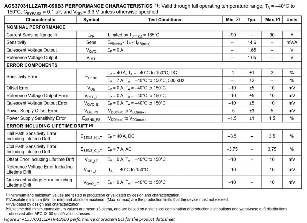
To illustrate how these methods diverge in practice, consider a real-world error budget based on the ACS37031 90 A current sensor. Before the terms are combined, all errors must be converted to a common unit: percentage of full scale (% FS). For a 90 A measurement range with a sensitivity of 14.6 mV/A, the full-scale analog voltage swing is 1314 mV. With the datasheet maximum, a 10 mV initial offset translates to a 0.76% FS error, and a 5 mV power supply offset becomes a 0.38% FS error. These combine with the specified 2.00% initial sensitivity error, 1.50% lifetime sensitivity drift, and 1.50% power supply sensitivity error differently depending on the mathematical method chosen. A worst-case linear summation simply stacks every extreme value to yield a highly pessimistic 6.14% error bound, which is guaranteed to be the absolute worst-case number for strict functional safety. However, treating these terms as independent variables and calculating the RSS yields a more realistic 3.04% error, representing the typical performance that a population of sensors actually delivers in the field.
- Worst-case (linear sum): 2 + 1.5 + 1.5 + 0.76 + 0.38 = 6.14%
- Root-sum-of-squares (RSS): √(22 + 1.52 + 1.52 + 0.762 + 0.382) = 3.04%
Conclusion
Achievement of high accuracy in a current sensing application is a systematic process to identify, quantify, and mitigate multiple sources of error. As detailed here, the total accuracy of a measurement is far more complex than a single percentage on a datasheet. It is a dynamic figure, dependent on the inherent characteristics of the sensor—such as sensitivity, offset, and linearity—and heavily influenced by external factors like operational temperature, stray magnetic fields, and system noise.
Deconstruction of accuracy into its fundamental components shows that a robust design requires a holistic approach. An engineer must not only select a sensor with low initial error but also consider how the system environment impacts its performance over time and temperature. The understanding that temperature drift can affect both sensitivity and offset, or that a nearby high-current cable can impose an external field, is the first step to create a truly reliable measurement system.
With the knowledge from this guide, you are now equipped to perform a comprehensive error budget analysis and to move from datasheet specifications to a real-world estimation of system performance. You can now make informed tradeoffs and implement specific design choices—such as how to provide stable power supplies or careful PCB layout—to minimize the total error.
With foundational elements of technology, architecture, and accuracy now addressed, the last step is to ensure that the sensor can operate reliably and to protect the system in a high-voltage environment. The next and final document in this series, “Robustness and Speed: A Guide to Isolation and Dynamic Performance in Current Sensors,” explores the critical topics of galvanic isolation and dynamic response and completes your journey to a comprehensive current sensing solution.
This document is part of a comprehensive series that provides guidance about current sensor selection. For additional content in this series, refer to Beyond the Datasheet: Mastering Current Sensing Selection.