From Amps to Kiloamps: How to Select the Right Current Sensor Architecture and Manage Power Density

Introduction
As electrification scales from household appliances to massive traction inverters for electric vehicle (EVs), the “one-size-fits-all’ approach to current sensing is a thing of the past. To help designers navigate the critical tradeoffs between sensor technologies, this document discusses application specific design considerations for a system that integrates a current sensor.
This document is part of the comprehensive series Beyond the Datasheet: Mastering Current Sensing Selection, which provides guidance about current sensor selection. This series previously established that knowledge of the input current profile for the desired application and an appropriately matched sensing technology—Hall-effect or tunnel magnetoresistance (TMR)—are foundational to proper current sensor selection.
With the basic technology and required sensing range determined as previously discussed in this series, the next critical decision revolves around the physical implementation of the sensor. The choice of sensor architecture is driven primarily by the magnitude of the current that is to be sensed and the power density requirements of the application. In traction inverters and industrial motors, as system currents scale from single-digit amperes to hundreds or even thousands of amperes, multiple options are needed and a single solution is not always feasible. An integrated sensor that is perfect for a 50 A application is impractical for a 500 A application due to the additional heat generated by I²R losses. Conversely, in a 10 A design, a large core-based assembly designed for 1000 A is excessive and is not cost-effective.
This document helps designers navigate design considerations, advantages, and disadvantages of the current sensor architectures offered by Allegro—integrated, coreless, and core-based. The best practices for printed circuit board (PCB) layout and system design requirements are discussed. Adherence to these guidelines is recommended to ensure that the chosen sensor operates with optimal power-density performance and long-term reliability, regardless of current level.
Integrated Vs. Core-Based Vs. Coreless
The diverse portfolio of current sensors by Allegro MicroSystems is built on different architectures, each optimized for specific current ranges and application requirements. Knowledge of these architectures—including integrated conductor (Figure 1), core-based (Figure 2), and coreless (Figure 3) architectures—is a critical foundation to successful selection of a device that can handle the current levels of the target system, from 2 A to thousands of amperes.
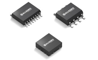
Figure 1: Integrated conductor current sensor packages
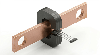
Figure 2: Core-based current sensor busbar implementation with single-inline package (SIP)
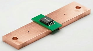
Figure 3: Implementations of coreless current sensing through busbar (top) and PCB current sensing (bottom)
What are the Current Limits of Integrated-Conductor Current Sensors
An integrated-conductor sensor represents a straightforward and compact current sensor implementation, where the current-carrying conductor is physically integrated into the integrated circuit (IC) package itself. Current flows directly through a leadframe path within the sensor package (Figure 4), and an internal Hall-effect or TMR element measures the resulting magnetic field.
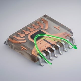
Figure 4: Integrated Conductor MA/LA package showing current flow through the internal conductor (leadframe) of the package
These devices are generally designed for current applications that need low-to-medium current levels, with a typical span of sensing ranges from less than 50 A (as low as 2 A) to approximately 400 A. The current-handling capability of an integrated sensor is limited by the thermal performance of the package. The resistance of the integrated conductor (typically from 100 µΩ to 1.2 mΩ) generates I²R heating. The package must be able to safely dissipate this heat without exceeding the maximum junction temperature of the silicon die. Current density is the ability of the sensor to move that heat into the PCB. This thermal constraint is the primary reason that these devices typically are not used for currents that exceed a few hundred amperes.
This architecture provides a simple, factory-calibrated, all-inone solution that does not require external magnetic components and that simplifies PCB layout. An integrated current sensor—such as the Allegro ACS37220, ACS71010, or ACS37030—offers a compact and convenient solution that simplifies the design and assembly process. Integrated current sensors are ideal for, but are not limited to, motor-control, load-detection, power-supply, and overcurrent fault-protection systems in automotive, industrial, and consumer applications. A few of the solutions offered in the Allegro integrated current sensor portfolio are summarized in Table 1.
| Integrated Current Sensor | Maximum Sensing Range [A] | Package Designator | Primary Conductor Resistance [mΩ] | VISO Isolation Rating [VRMS] |
|---|---|---|---|---|
|
±50 |
LZ (custom SOIC-6) |
0.68 |
3500 |
|
|
±50 |
LC (SOIC-8) |
1.2 |
2400 |
|
|
±65 |
LZ (custom SOIC-6) |
0.68 |
3500 |
|
|
±65 |
MY (custom SOIC-6) |
0.9 |
4242 |
|
|
±65 |
TMR SOIC-8 |
1 |
3500 |
|
|
±65 |
TMR SOIC-16 |
1 |
5000 |
|
|
±65 |
LA (SOIC-16) |
1 |
4242 |
|
|
±80 |
MA (SOIC-16) |
0.85 |
5000 |
|
|
±80 |
MC (SOICW-16) |
0.625 |
5000 |
|
|
±200 |
EZ (custom 4 x 4 mm QFN) |
0.1 |
100 (functional) |
|
|
±400 |
CB (custom 3-pin module) |
0.1 |
4800 |
When Should a Core-Based Current Sensor be Used Instead of an Integrated Current Sensor?
When system requirements exceed 400 A, magnetic concentrators should be used. To measure very high currents, a core-based approach is used. In this architecture, the sensor IC does not carry the primary current. Instead, a standalone Hall-effect sensor IC, such as the ACS37600 or ACS70312, is paired with an external ferromagnetic core. The primary conductor (such as a busbar) passes through the center of this core. The core concentrates the magnetic field generated by the current and guides this magnetic field to the sensor, which is placed within a small air gap in the core. These SIP-packaged Hall-effect sensors translate high-magnitude primary current into an analog output. The ferromagnetic concentrator simultaneously maintains physical isolation from the high-current bus. This topology not only facilitates large currents, but also inherently shields against the external magnetic fields that are typical of applications with fast-switching environments. When paired with the high-bandwidth, low noise signal paths of Allegro technology, core-based designs enable high-current applications.
The sensing range is not limited by the sensor IC itself; rather, it is determined by the design of the external magnetic core. This makes the architecture flexible and enables measurements from ten amperes, to hundreds of amperes, to well over thousands of amperes. Use of a ferromagnetic core to concentrate the magnetic field produced by the current enables a core-based sensor that can measure significantly higher current than an integrated conductor solution. Compared to an integrated conductor solution, the core based approach requires an additional external component (the core), which adds cost, size, and weight to the overall system. System accuracy also depends on the magnetic properties of the core material, which can exhibit thermal drift and hysteresis, and the design must account for these effects.
While a core-based current sensor is a good solution for accuracy and inherent magnetic shielding, it introduces physical and performance tradeoffs. The primary drawbacks arise from bulk and mechanical complexity: The ferromagnetic core adds substantial size, weight, and cost to a design. Due to core saturation and hysteresis, residual magnetism after a high-current surge can leave the sensor with a permanent offset error, which creates a “magnetic ceiling” for this solution. A core-based design is also inherently limited by eddy currents within the metal concentrator, which restricts the usable bandwidth of the sensor.
A core-based solution provides a robust and effective method to measure very high currents, far beyond the thermal limits of an integrated package, while also providing inherent galvanic isolation. The core-based approach enhances sensor sensitivity and allows for the measurement of very high currents with high accuracy. Core-based current sensing is ideal for applications that require galvanic isolation, high-current levels that exceed 200 A to 400 A, and high accuracy, such as EV traction inverters and industrial motor drives. A few of the core-based solutions offered by Allegro are summarized in Table 2.
| Core-Based Current Sensor | Typical Current Range [A] | Sensing Range [mV/G] | Bandwidth [kHz] | Package |
|---|---|---|---|---|
|
200 to 1000+ |
–18 to 18 |
400 |
8-pin TSSOP package (suffix LU) |
|
|
200 to 1000+ |
–7.2 to 7.2 |
400 |
4-pin SIP (suffix KT or OK) |
|
|
200 to 4000+ |
0.5 to 11.5 |
240 |
4-pin SIP (suffix KT or OK) |
|
|
200 to 1000+ |
0.5 to 1.8 |
240 |
4-pin SIP (suffix KT) |
|
|
200 to 1000+ |
0.6 to 14 |
120 |
4-pin SIP (suffix KT) |
When are Coreless Solutions Used for High-Current Applications and Contactless Measurements?
Coreless sensing is an innovative architecture that provides the high-current measurement capability of a field sensor without the need for a bulky external core. In this contactless design, a highly sensitive, differential Hall-effect sensor IC, such as the ACS37610 or ACS37612, is placed in close proximity to a current-carrying busbar or a wide PCB trace. The sensor directly measures the magnetic field produced by the current that flows through the conductor. Similar to the core-based approach, the sensing range is highly flexible and is determined by the geometry of the external conductor (shape and size) and its distance from the sensor IC. This architecture is well-suited to measure currents from 100 A to over 4000 A. This flexibility allows the sensor to be adapted to a wide range of current levels.
The performance of a coreless system is highly dependent on the mechanical precision of the assembly. This is because the distance and alignment between the sensor and the busbar directly impact the measurement sensitivity. While the Allegro differential sensing technology provides excellent rejection of stray magnetic fields, careful system design is required to shield the sensor from significant external magnetic interference. A coreless architecture achieves the highest power density. In a coreless architecture, the sensor is decoupled from the heat source and the bulk of a magnetic core is eliminated. Unlike an integrated sensor, where current flows through the IC package, a coreless sensor is placed in close proximity to an external busbar, which allows the conductor itself to act as a massive heat sink for conductive losses. In a coreless architecture, the absence of the entire ferromagnetic concentrator drastically reduces the total system volume and allows a tiny surface-mount technology (SMT) package to measure thousands of amperes without core saturation limits or thermal bottlenecks.
While a coreless solution offers the highest power density and eliminates core-related issues like saturation and hysteresis, it trades off the built-in physical protection provided by a concentrator from external magnetic interference. The primary drawback is its susceptibility to external stray fields: Without a ferromagnetic core to act as a shield, a coreless sensors must rely on differential sensing techniques to cancel out magnetic noise from nearby motors or busbars. To ensure signal integrity in environments with high electromagnetic interference (EMI), placement and PCB orientation are much more critical during the design phase. This method eliminates the cost, size, and weight of a magnetic core and thereby enables a high-current sensing solution that is smaller and lighter than a core-based solution. A coreless current sensor provides a galvanically isolated, noncontact method to measure current: It senses the magnetic field generated around a conductor and offers a noninvasive, lossless measurement for high-power systems.
A few of the coreless solutions offered by Allegro are summarized in Table 3.
| Coreless Current Sensor | Typical Current Range [A] | Sensing Range [mV/G] | Bandwidth [kHz] | Package |
|---|---|---|---|---|
|
100 to 4000+ |
5 to 15 |
250 |
8-pin TSSOP (suffix LU) |
|
|
100 to 4000+ |
5 to 15 |
250 |
8-pin TSSOP (suffix LU) |
|
|
200 to 1000+ |
2.5 to 20 |
240 |
8-pin TSSOP (suffix LU) |
Power Density/Thermal Management
Power density, which refers to the amount of power a device can handle per unit volume or footprint, is an increasingly important consideration in the selection of a current sensor. In modern electronic designs, there is a growing demand for smaller, more-efficient components that can deliver high performance without excessive heat generation. High power density is not just about handling power, it is also about the efficiency of heat removal. High power density in a current sensor impacts several critical aspects of system design and operation, and a higher power density indicates that the sensor can handle and dissipate more power in a smaller package, which is particularly valuable in space-constrained applications.
Why Does Power Density Matter?
Power density is the defining factor in modern power electronics design. As systems transition to wide-bandgap (WBG) semiconductors like SiC and GaN, the ability to manage high power in minimal space is essential for performance.
As previously mentioned, power density management is a primary factor for integrated current sensors. The power density is limited by the internal primary conductor resistance (typically IPR) and the ability of the package to dissipate heat into the PCB. Because the current flows directly through the IC, I2R losses occur directly inside the device due to resistive dissipation. To minimize heat generation and to maintain high power density, Allegro uses ultralow-resistance leadframes (down to 100 μΩ) and high-conductivity copper. Knowledge of self-heating is critical because it directly impacts both the accuracy and the reliability of a current sensor. When current passes through the resistive path of an integrated sensor, the resulting heat increases the internal junction temperature of the silicon die; without proper heat management, a thermal drift can occur, where sensor offset and sensitivity shift away from the factory-calibrated values. This leads to measurement errors. Furthermore, excessive self-heating can push the device beyond its safe operating area (SOA), which has the potential to permanently damage the product or shorten the product lifespan.
Size Reduction and Footprint Optimization
Higher power density allows for a reduction in the physical volume of the IC and the overall system. In automotive applications, where space is at a premium, increased power density enables smaller PCBs and more-compact end products. This allows for a more-efficient use of space without sacrifice to power-handling capabilities.
Cost Efficiency Through Dematerialization
An increase to the power density of a high-current path directly reduces the total bill of materials (BOM). By handling more current per square millimeter of PCB, designers can use smaller enclosures and reduce the overall surface area of the circuit board. This dematerialization (smaller BOM and smaller overall footprint) leads to lower costs for substrates, materials, and protective potting compounds, which is critical for high-volume manufacturing.
System Integration and Thermal Isolation
Sensors are increasingly placed into crowded environments alongside microcontrollers and power stages. High power density enables a sensor to fit into tight footprints and maintain thermal isolation. Use of a sensor with low-resistance leadframes minimizes I2R losses.
Parasitic Inductance and Switching Efficiency
High-power-density layouts naturally result in shorter physical distances between components. In high-speed switching environments (using SiC or GaN), this reduction in distance is vital to lower the parasitic inductance of the PCB traces and busbars. Minimized loop inductance is critical to reduced voltage ringing and overshoot during high dI/dt events. This allows the system to operate at higher frequencies with lower switching losses, which improves the overall converter efficiency and protects the sensor from EMI.
Power Density for Core-Based Solutions with an External Concentrator
A core-based sensor uses a ferromagnetic core to concentrate the magnetic field generated by the current. The sensor itself is physically and thermally isolated from the high-current path. This allows for extremely high power density at the system level because the sensing part of the circuit does not become heated from the primary current. While the sensor itself might not have a high power density, the design of the conductor can significantly impact the overall system power density. A smaller conductor increases power density, and a larger conductor reduces power density. Although the sensor itself does not directly dissipate much power, the conductor can generate significant heat, especially at high currents. Proper thermal management of the conductor is essential. While the sensor is safe, the core can become a heat source due to eddy-current losses at high frequencies. The core material can saturate at high currents, which leads to nonlinearity and reduced accuracy. Careful selection of the core material and dimensions is crucial to avoid saturation and heat.
Power Density for Coreless Solutions and the Contactless Approach
In contrast with a core-based solution or a physical connection like an integrated-conductor current sensor solution, a coreless sensor measures magnetic field directly from a PCB trace or busbar without a concentrator. This architecture offers the highest possible power density. Because physical contact does not occur and a core is not present to saturate or heat, the primary current is only limited by the physical dimensions of the busbar or PCB trace.
The sensor is contactless, meaning there is a controlled air gap or dielectric layer between the high-voltage/high-current path and the low-voltage sensor. This provides galvanic and thermal isolation. Because the sensor is coreless, it is susceptible to external stray fields. Allegro uses differential Hall elements to reject common-mode fields. This approach ensures that a high-power-density layout (where components are packed closely) does not result in measurement interference. The heating and power density behavior for each type of Allegro current-sensing solution is summarized in Table 4.
| Feature | Integrated | Core-Based | Coreless |
|---|---|---|---|
|
Typical Current Range |
2 A to 400 A |
20 A to 1000+ A |
100 A to 4000+ A |
|
Sensing Method |
Current passes through the sensor; all-in-one solution, but has the highest thermal bottleneck |
Current passes near the part, but the magnetic field is “captured” and “shaped” by a physical core; accurate but bulky |
Sensor is placed above or near the conductor; physical contact does not occur; bulky core is not present; greatest-power-density and lightest-weight solution for high current |
|
Primary Advantage |
Smallest footprint; factory calibrated for ease of use |
High accuracy; inherently shielded from external fields by core |
Lossless; lowest cost for very high currents; magnetic/core saturation does not occur |
|
Primary Disadvantage |
Thermally limited by I2R losses in the package |
Bulky, heavy, costly, and susceptible to magnetic-core saturation/ hysteresis |
Sensitive to mechanical alignment, PCB/busbar design, and external stray fields |
|
Isolation Type |
Inherent galvanic isolation; level depends on package |
High galvanic isolation; determined by core and conductor spacing |
Inherent (noncontact); depends on air gap/insulation of conductor |
|
Bandwidth |
High: 100 kHz to 1 MHz (TMR versions up to 5 MHz) |
Low-medium: limited by eddy-current losses in the core |
High: limited by sensor |
|
Accuracy/Drift |
High (factory programmed) |
High (must account for core thermal drift and hysteresis) |
System-dependant (system-level calibration for best results) |
|
Power Dissipation |
Highest: conducts current through internal leadframe |
Negligible: sensor IC is isolated; core losses are minimal |
Negligible: IC consumes very little power; current remains in busbar or PCB |
PCB Layout Best Practices
In high-performance power electronics, the PCB is an important consideration. To ensure the accuracy, safety, and long-term reliability of a current sensing solution, adherence to PCB layout best practices is essential. Because a current sensor relies on precise magnetic-field measurement, a minor layout deviation can lead to a measurement error or a thermal failure. Adherence to established design guidelines can minimize parasitic resistances and inductances, maximize power density, and ensure that the sensor operates within its calibrated thermal limits. Furthermore, it is always necessary to conduct bench measurements in application to verify that the final system meets thermal needs.
Integrated Current Sensor Layout Best Practices
For integrated current sensor solutions, the PCB serves as the primary heat sink for the power dissipated as heat through the internal leadframe. The cross-sectional area of the copper traces is the most important factor in the reduction of thermal resistance of the system. Therefore, to manage these losses effectively, a designer should prioritize maximized copper volume by use of the thickest copper practicable, typically in the range of 2 oz to 4 oz. Additionally, incorporation of an array of thermal vias directly below the high-current pins and the thermal pad is essential; these vias connect the top-layer solder lands to internal and bottom copper planes to spread heat away from the sensor junction. Properly matched trace widths are also critical; to prevent thermal bottlenecks that significantly increase local temperature rise, the input and output traces should be at least as wide as the sensor high current pins. Finally, expansion of the solder lands beyond the minimum requirements of the insulation piercing connector (IPC) provides larger pads that increase the surface area available for both convective and conductive cooling.
Core-Based Sensor Layout Best Practices
In a core-based design, the sensor is typically isolated from the high-current path, but the layout must still prioritize mechanical and magnetic stability. During operation, even though the sensor is contactless, the busbar generates heat. It is essential to size the busbar appropriately to limit the temperature increase at the sensor location, which prevents thermal drift in magnetic sensitivity. Furthermore, the layout must ensure that the sensor remains perfectly centered within the gap of the concentrator. Use of rigid mounting or high glass-transition-temperature PCB materials helps prevent the board from the high-temperature warpage or shifts that would otherwise cause measurement errors. Finally, a magnetic keep-out zone maintained around the core is critical; to prevent magnetic interference and saturation, high-current traces or other ferromagnetic materials, such as steel screws or components, should not be placed near the core.
Coreless Solutions Layout Best Practices
A coreless sensor is highly sensitive to layout geometry because it lacks a concentrator to shield it from external fields. To maximize common-mode field rejection, high-current traces should be routed symmetrically relative to the differential Hall elements of the sensor. This ensures that external fields affect both Hall plates equally and are subtracted by the internal logic of the sensor. Additionally, to mitigate stray field effects, the sensor should be placed as far as practicable from other high-current traces, and it should be oriented so that its sensitive axis is orthogonal to magnetic-field interference. An integrated sensor has internal isolation defined by the package; a coreless/core-based sensor has isolation determined by the PCB/busbar design.
Conclusion
Selection of the proper current sensor architecture is a critical design step that balances performance, size, cost, and thermal constraints. As discussed in this document, the magnitude of the system current is the primary factor that drives this selection. For an application with typical current of less than 200 A, an integrated current sensor offers a compelling solution in a compact, fully calibrated, easy-to-integrate package. The primary design consideration of an integrated current sensor is thermal management: To maintain accuracy and reliability, the design must ensure that the I²R losses inherent in the integrated conductor dissipate effectively through the PCB.
When current exceeds the practical limits of an integrated solution, coreless and core-based architectures provide robust, contactless alternatives. A coreless sensor offers excellent flexibility and high-level galvanic isolation, which makes it ideal for a design where a busbar or PCB trace already routes high current. For applications that demand the utmost accuracy and immunity to external magnetic fields, the superior choice is a core-based sensor that uses a magnetic concentrator. Ultimately, architecture selection is not just about current measurement; it is about management of the physical realities of power and heat. By use of a sensor architecture correctly matched to the current level of the application and implementation of sound thermal-design practices, an engineers can build a robust foundation for a high-performance power system.
Key Takeaways
- Current Dictates Architecture: The choice between an integrated, coreless, or core-based architecture is driven primarily by the continuous current and the resulting thermal limits of the system.
- Integrated is for Simplicity: For applications that require less than 200 A, an integrated-conductor sensor (like the ACS37220 or ACS71010) provides a factory calibrated, “plug-and-play” solution with the smallest footprint.
- Coreless for Maximum Power Density: For measurement of 100 A to 4000+ A within a tight space, a coreless differential sensor offers a lossless, contactless method that eliminates bulky magnetic cores. The tradeoff is mechanical tolerance. A shift in busbar placement can result in a sensing error.
- Core-Based for Harsh Environments: If the design requires high accuracy and immunity to external magnetic stray fields at very high current, a core-based solution with a ferromagnetic concentrator is a good solution.
- Layout is a Critical Component: Regardless of the architecture, the PCB or busbar design acts as both a magnetic interface and a thermal heat sink. For long term reliability, adherence to the best practices for copper volume and thermal vias is essential.
- TMR is the High-Speed Frontier: For applications that require bandwidth up to 5 MHz, an Allegro TMR based integrated sensor offers a significant performance improvement compared to traditional Hall-effect technology. TMR also offers better sensitivity, which can allow for even smaller integrated packages or better performance at lower current levels within a high-current architecture.
| Feature | Integrated | Core-Based | Coreless |
|---|---|---|---|
|
Typical Current Range |
2 A to 400 A |
20 A to 1000+ A |
100 A to 4000+ A |
|
Sensing Method |
Current passes through the sensor; all-in-one solution, but has the highest thermal bottleneck |
Current passes near the part, but the magnetic field is “captured” and “shaped” by a physical core; accurate but bulky |
Sensor is placed above or near the conductor; physical contact does not occur; bulky core is not present; greatest-power-density and lightest-weight solution for high current |
|
Primary Advantage |
Smallest footprint; factory calibrated for ease of use |
High accuracy; inherently shielded from external fields by core |
Lossless; lowest cost for very high currents; magnetic/core saturation does not occur |
|
Primary Disadvantage |
Thermally limited by I2R losses in the package |
Bulky, heavy, costly, and susceptible to magnetic-core saturation/ hysteresis |
Sensitive to mechanical alignment, PCB/busbar design, and external stray fields |
|
Isolation Type |
Inherent galvanic isolation; level depends on package |
High galvanic isolation; determined by core and conductor spacing |
Inherent (noncontact); depends on air gap/insulation of conductor |
|
Bandwidth |
High: 100 kHz to 1 MHz (TMR versions up to 5 MHz) |
Low-medium: limited by eddy-current losses in the core |
High: limited by sensor |
|
Accuracy/Drift |
High (factory programmed) |
High (must account for core thermal drift and hysteresis) |
System-dependant (system-level calibration for best results) |
|
Power Dissipation |
Highest: conducts current through internal leadframe |
Negligible: sensor IC is isolated; core losses are minimal |
Negligible: IC consumes very little power; current remains in busbar or PCB |
This document is part of a comprehensive series that provides guidance about current sensor selection. For additional content in this series, refer to Beyond the Datasheet: Mastering Current Sensing Selection.