Guidelines for Designing Subassemblies Using Hall-Effect Devices
By John Sauber and Bradley Smith, Allegro MicroSystems, LLC
Introduction
The Hall effect, discovered by E. H. Hall in 1879, is the basis for all Hall-effect devices. When this physical effect is combined with modern integrated circuit (IC) technology, many useful magnetic sensing products are possible. The Hall element, when properly biased, produces an output voltage that is proportional to a magnetic field. This small voltage is processed through a high-quality amplifier, which produces an analog signal that is proportional to the applied flux density. In Allegro® Hall-effect devices, the signal is conditioned and optimized for various types of magnetic inputs to produce a suitable electrical output.
Hall-effect elements respond to stress by modifying the output voltage versus the magnetic flux-density curve. For this reason, it is important that designers, from chip to final customer, understand that environmental stress from thermal or mechanical sources can affect the output of a Hall-effect element. The chip designer anticipates the end use, builds compensation circuits, and connects multiple Hall elements in such a manner as to minimize the effects of the anticipated environment. When the proper IC design is matched with the proper package design, environmental effects are minimized.
Although robust design techniques greatly reduce the effects that package stresses may place on the operation of the Hall-effect IC, it is important that assembly manufacturers take precautions to avoid unnecessary external stresses such as those caused by overmolding, gluing, welding, lead bending or forming,lead clipping or trimming, or clamping.
In addition to avoiding stresses which affect the electrical parameters, it is also essential to avoid stresses which could introduce any reliability risks. This application note provides design guidelines for subassemblies to avoid both of these problems.
While this document covers most of the assembly methods used for mounting Hall-effect devices, it does not cover soldering to conventional circuit boards. For information on that subject, refer to Soldering Methods for Allegro Products (SMD and Through-Hole) on the Allegro website.
Stress-Sensitive Locations
There are several locations on a package which are vulnerable to stress, as shown in figure 1. Regardless of the method used for building a subassembly, it is important to minimize the stress in these areas.
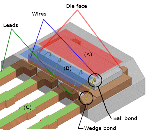
Figure 1. Stress-sensitive locations. (A) Force over die face can cause die cracking and parameter shift. (B) Force over wires can cause damage to wedge or ball bonds. (C) Force or bending applied to leads can damage wedge bonds and cause package cracking.
Failure Modes
The locations shown in figure 1 are associated with the following failure modes:
(A) Forces over the die face can cause cracking of the die. The die may fail immediately, or it may have a crack which is a latent defect. See the Design Validation Testing section for information on finding latent defects. Forces over the die can also cause electrical parameter shift. If force must be applied to the die face, it should be distributed evenly over the entire top surface.
(B) Forces over the gold bond wires can damage the ball bond (on the die-end of the wire) or break the wedge bond (on the leadframe end of the wire). These wires are extremely small, having a cross-sectional area that is approximately one-ninth that of a human hair (see figure 2). The "neck" of the wedge bond is even smaller, being about one-fourth of the cross-sectional area of the wire. Any deformation or movement of the molding compound relative to the wire can cause damage, as shown in figure 2 (right panel). Again, it may cause an immediate failure or a latent defect.
(C) Forces or bending moments applied to the leads can cause damage to the wedge bonds (possibly a latent defect), or package cracking.
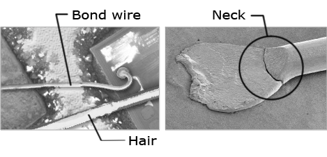
Figure 2. (Left) Gold bond wire (Ø0.025 mm) has approximately one-ninth the cross-sectional area of a human hair (Ø0.076 mm) and is very fragile. (Right) The "neck" thickness of the wedge bond is approximately one-fourth that of the bond wire, and is the most likely point of failure.
Inside of the package, only a small portion of the leads is embedded into the molding compound. In the case of the K package, shown in figure 3, only 0.8 mm of the leads, which are 15.5 mm long, is inside of the molding compound. The resulting lever arm amplifies the force on the lead by a factor of nineteen so that even a small force can damage the wedge bonds. Because of this, it is important to follow the lead clamping guidelines during lead forming, and to avoid forces on the leads during other processing steps.
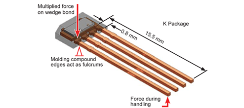
Figure 3. It is important to clamp the leads before any lead-forming operations. Because of the leverage effect, even a small load applied to the end of the lead is multiplied (in this package, by 19 times), and produces a large load at the wedge bond.
Forming Leads
Lead-forming operations at the customer facility are often a necessary part of preparing Hall-effect devices for use in applications. For most Allegro devices, the few simple precautions described in the next section, Standard Forming Procedures, will ensure that lead-forming does not induce damaging stress to the leads, the epoxy case, or the internal IC. While these precautions should always be taken into consideration, exceptions exist for certain Allegro gear tooth sensor IC (ATS) packages with enhanced lead support. The exceptions are described in section titled Considerations for ATS Packages following.
Standard Forming Procedures
A few simple precautions will ensure that lead-forming does not induce damaging stress to the leads, the epoxy case, or the internal IC.
- Leads should not be formed or clipped closer than 0.76 mm to the package case, and they must be supported from above and below, so that no movement or stress can occur in this area during the lead-forming operation (see figure 4).
-
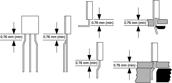
Figure 4. Setup for leadforming operations.
- The lead-former should clamp the leads sufficiently (top and bottom) so that there is no force trying to pull the leads from the epoxy package case during the forming process. It is best to physically isolate the package body during lead forming, so that no force can transfer to it.
- All bends must be made over a smooth anvil with a radius of at least one-half the lead thickness.
- Leads should not be deformed in the bend area by squeezing the leads between the former and the anvil. Spring-back must be eliminated by over-bending, not by deformation.
- Less stress is transferred to the package if a roller forming tool is used rather than a push-rod. Roller forming is the preferred method to use.
- Lead-forming may result in tooling marks on the lead surface. These are acceptable as long as the marks are not severe enough to penetrate the plating and expose the leadframe base metal.
Considerations for ATS Packages
Certain Allegro gear tooth sensor IC (ATS) packages are designed so that they can incorporate the Hall sensor IC with other components, such as a pole piece or back-biasing rare-earth pellet, as an optimized device.
For lead-forming of SA and SB packages, Allegro recommends that all of the recommendations in the Standard Forming Procedures section be followed.
The SE, SG, SH, and SJ packages have a molded lead bar (figure 6) that holds the leads coplanar and in position during shipping and handling. Leave the molded lead bar attached during the lead-forming operation. Do not remove the bar until all forming of the leads is complete. This will prevent the leads from spreading apart and will optimize lead planarity and spacing.
Figure 6. Molded lead bar used to constrain leads on some packages for handling.
Inspection criteria for sufficient clamping
As mentioned in the previous sections, the lead must be clamped sufficiently to prevent pulling on the leads during forming. Inspecting the "witness marks" left in the plating can show whether or not the clamping was adequate.
- The top side of the lead should have even clamping marks in the plating. The marks should:
• show uniform clamping across most of the width of each individual lead, and
• show the same shape and depth of clamping across all of the leads. - The bottom side of the lead should also have uniform clamping marks. As an additional criterion, the die burr (an artifact of stamping) on the bottom of the lead should be flattened out. If the burr is not flattened, the clamping force was not sufficient.
- The clamping force should NOT be so great that it changes the cross-sectional shape of the base metal, or leaves any visible damage to the molding compound.
High Temperature Handling Precautions
Thermoset molding compounds, which are used for the Allegro package body, have a glass transition temperature, Tg, which is typically between 140°C and 160°C. When the compound is heated above its Tg level, it experiences a very significant reduction in its strength. Because of this, when the temperature of any process exceeds Tg, care must be taken not to apply loads to any of the locations shown in figure 1.
In addition to low strength above Tg, the molding compound also experiences viscoplasticity (creep), which allows the compound to deform slowly over time. Care must be taken not to deform the leads so that they become "spring-loaded," because subsequent high-temperature processing can result in lead movement, which also can result in damage to the wedge bonds.
General Precautions for Soldering and Welding
When a process requires that a formed lead be soldered or welded, there are three main rules to keep in mind:
- Not too short – If possible, it is best to avoid extremely short leads. A longer lead is bent without creating high forces. This allows for alignment and forming tolerances, and also reduces stresses from any expansion mismatch with the leadframe that it is soldered to.
- Not too hot – As mentioned above, the strength of the molding compound is greatly reduced at high temperatures. Soldering and welding operations should be done at the lowest temperature and in the shortest time possible. Using a longer lead also minimizes the amount of heat which reaches the device case.
- Not "spring-loaded" – Although forming and alignment tolerances mean that leads will usually need to be deformed slightly during welding or soldering, the less deformation the better. If a lead must be significantly bent when it is attached in the application, spring energy will likely be stored in the lead. Any subsequent high temperature processing (such as overmolding) or prolonged exposure to high temperature operating environments may cause the lead to move within the molding compound, resulting in wedge bond failure.
If there are concerns that a given process or design may be creating high stresses in the leads, which could be causing a reliability risk, refer to the Design Validation Testing section for information on methods for finding latent defects.
Soldering of Leads
In addition to the information in this application note, refer to Soldering Methods for Allegro Products (SMD and Through-Hole), on the Allegro website. That includes guidelines on lead finishes, solders, fluxes, contaminants to avoid, and general processing parameters.
Welding of Leads
As described in this section, welding should be approached with careful attention, planning, and process testing because of the small geometries of the device cases and plating. There are two welding methods that have been used with success, conventional resistance welding, and a type of welding process called tin-fusing (Sn-fusing). The choice of process may be determined by the application and by production conditions.
Tin-fusing Versus Resistance Welding
- Resistance welding involves heating the parts to be joined until the base metal (copper) is in a plastic state, and then forging the parts together.
- Tin-fusing involves vaporizing a thin layer of tin plating, which produces ultra-clean base metal surfaces. An application of pressure then results in an extremely strong diffusion bond between the two parts. This is the preferred process.
- Most types of conventional resistance welding equipment can also be used for tin-fusing, the difference is that much lower voltages and currents are used.
Advantages of Tin-Fusing
Tin-fusing may have advantages over resistance welding for small electronic devices:
- It is very difficult to resistance-weld copper to copper without destroying the part.
- Tin-fusing causes less deformation of the leads than welding because it is quicker and because melting the base metal is not required.
- Tin-fusing creates a diffusion bond of base metal to base metal, which is often stronger than the bond created by welding (for copper to copper).
Guidelines for Tin-Fusing
- Reducing the current level used is a process advantage. Tin-fusing requires much less current than resistance welding. To avoid overheating the device, the lowest current which creates a reliable bond should be used. This also reduces the cost of the electricity required. Figures 7 and 8 are examples for comparison.
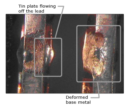
Figure 7. Damage caused by excessive heat during welding, which includes deformation of the base metal and flow of the tin plating. It was welded at 1700 A, 1.0 V, for 11 ms.
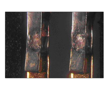
Figure 8. Leads welded with a lower current level (1100 A, 0.8 V, for 10 ms). There is very little damage, and the pull strength of the joint is essentially the same as the overheated leads in figure 7.
- Avoid short leads because they can cause the following problems:
- Welding can flatten out leads, and if the leads are very short then the flattened area can damage the molding compound. Also, the lateral movement of the lead that occurs when it is flattened close to the package case can damage the wedge bonds or cause a short between the leads (see figure 9).
- Welding operations create high temperatures which can damage the package body if the leads are too short.
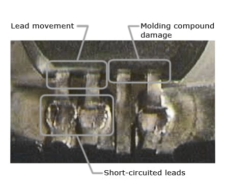
Figure 9. Damage caused by lead flattening resulting from welding leads that are too short.
- Ideally, tin-fusing should be used with approximately 100% tin plating. The presence of lead (Pb) does not affect the quality of the bond, but the processing of Pb does create a potential environmental health risk. During tin-fusing, the plating in the area of where the two pieces touch is vaporized. For a typical weld with Allegro parts, this would release less than 2 µg of Pb. The Pb vapor must be collected and disposed of in a safe and environmentally responsible manner.
- Many types of copper alloys can be successfully welded. The best choice should be determined by the supplier of the welding equipment.
- In general, alloys containing iron, such as Kovar or Alloy 42, should be avoided because they are difficult to weld to a copper leadframe with tin plating.
Laser Welding
Welding tin-plated copper leads onto a copper leadframe is possible, using a laser. The considerations are similar to tin fusing; thus, avoiding excessive power is important. "Dry" welding can be used, but solder paste can also be used and can provide better solder fillets, to make a stronger joint. Because a laser spot is focused to a very small area, care must be taken to ensure that the resulting bond surface area is sufficient to make a strong bond.
Allegro Lead Plating
Allegro has taken steps to provide a good tin plate for tin-fusing welding. The typical industry standard for plating thickness mean is 14 µm but Allegro has chosen a standard mean thickness of 11.5 µm. This reduced thickness allows better control of the plating bath parameters and gives a superior quality finish with excellent solderability. It is also better for tin-fusing because there is less tin to melt, so spattering is controlled.
Attaching the Device to the Subassembly
Most gluing, coating, potting, or encapsulation methods add stress to the package, which can result in electrical parameter shift and scatter.
Gluing
Gluing a device into a cavity in a manufactured subassembly is a common method of assembling a Hall effect interface. The basic rules are:
- Match the expansion characteristics of the glue or molding epoxy as closely as possible to the component epoxy, which has an expansion rate of 12 to 30 ppm/°C. Most highly-filled (non-conductive) epoxies fit into this category and usually are good choices.
- Surface-mount component mounting epoxies can also be used to attach molded components. These materials do not match the Hall-device characteristics as well as filled epoxies, but have the advantage of being effective in very tiny dot sizes and they have a fast cure time.
- Cyanoacrylate ( "super glue" ) is not a good choice for gluing Hall-effect devices because it has a high rate of shrinkage when it cures. If the glue is applied to only one side of the device, this shrinkage can bend the device and cause severe stress. These glues also tend to be biodegradable and can dissipate in many common environments.
Conformal Coating
A conformal coating is often used to provide both protection from the environment, as well as some amount of mechanical protection. For keeping out contaminants, the key properties are water vapor transmission rates and oxygen permeability. Based on these criteria, the best choices are (in order):
- Urethane acrylic
- Epoxy
- Silicone
Plastic encapsulation (direct overmolding)
Fully encapsulating Hall-effect devices by overmolding with either thermoset or thermoplastic materials can cause parametric shift. Hall-effect devices encapsulated in this way should be retested over the full range of temperatures dictated by the application. The temperatures required for molding thermoplastics are usually above the reflow temperature of the plating on the leads, so the mold design must be such that the plating is not melted (tin melts at 232°C). If plating is melted during the mold process, it may flow against the body of the device and electrically short-circuit adjacent leads.
Cavity pressures in thermoplastic molds are very high. In general, pure hydrostatic pressure does not usually damage the device, as long as it is entirely inside the mold cavity. The mold design must be such that there are no bending forces applied to the Hall device during the molding process. Bending stresses can alter the device parameters and, if high enough, crack the die inside the epoxy package.
In situations where the Hall device forms a plug in an injection mold cavity with the device being held by the leads, it is important that the end of the device be supported. If there is clearance between the device and the end of the mold cavity, then the device can become a piston that is pushed forward in the mold cavity, pulling and stretching the leads.
The safest way to fully enclose a molded Hall-effect device is to design a housing (cap or sleeve) into which the device can slip-fit. The device can then be overmolded, potted, or glued into place. There are several considerations to keep in mind:
- Avoid any interference between the cap or sleeve and the leads. Any force applied to the leads can create spring loading, which can result in damage to the wedge bonds during overmolding, or prolonged high temperature operation.
- Press-fit applications are usually very tight and require a large force for insertion.Such forces can induce failures in the wires, wire bonds, or silicon IC, and should be reduced.
- Proper holding of the device during insertion is essential to minimize the forces acting upon the package. The flat face of the package (brand side) should never be clamped or impacted during insertion. The use of the sides and rear of the package is preferable during insertion.
Location of the overmold features can also be a concern:
- Minimizing the thickness of the overmold over the die face is an effective way to minimize the stress acting on the die, and the associated risks of die cracking and parameter shift.
- Avoid locating the gate for the overmold directly over the die because the thermal shock during molding can increase the risk of die cracking.
- Avoid locating the parting line of the mold over the die face if possible. Due to mold-half misalignment, this can sometimes create a "step" in the overmold, which can act as a stress concentrator over the die, and (possibly) increase the risk of die cracking.
- Avoid locating an ejector pin over the die face because this is very likely to cause die cracking.
Either thermoset or thermoplastic materials can be used. Selecting a material with the following attributes can minimize the stress and the risk of parameter shift or damage to the die:
- Low coefficient of thermal expansion (CTE)
- Low Elastic Modulus
- Low molding temperature
Most overmold materials are NOT hermetic, and will not completely protect the device from infiltration of contaminants. This is of particular concern in automotive applications where the assembly may be exposed to harsh environments and to substances such as automatic transmission fluid (ATF), salt water, and brake fluid. The use of a conformal coating, prior to overmolding, can stop moisture ingress and greatly reduce risks, but not eliminate them.
Potting
Potting is one of the best ways to assemble without inducing stress. When selecting a potting compound, the material should have the same attributes as listed above for overmolding materials, namely: low CTE, low modulus, and low cure temperature.
Potting with resilient materials, such as RTV silicones or urethanes, can reduce stress. However, when the resilient materials are enclosed in a housing, it is still possible for stresses to result due to differences in the coefficient of thermal expansion. Resilient materials typically have high expansion rates. For this reason, it is important to either leave one end of the container used for potting open, or at least leave some air space inside to allow room for expansion.
Potting with resilient foams is an excellent way to control stress from thermal expansion and still enclose the component. If the foam used is open cell, a sealer will be required to prevent the foam from filling with moisture.
Ultrasonic Welding
Any ultrasonic welding of plastics in close proximity to the Hall-effect device must be done with caution to avoid work-hardening of the copper base material in the leads and possible breakage of the internal leads. Direct contact between the package or leads and the ultrasonic welding "horn" should be avoided.
Also, as previously mentioned, it is important not to bend the leads during a soldering or welding operation so that they are "spring-loaded." If bending or tensile stresses are stored in the lead, and then ultrasonic energy is applied, it can result in damage to the leads or to the wedge bonds inside the package.
Note: Regardless of what assembly methods are used, it is essential to perform empirical testing to evaluate the effects of stress-induced parameter shift in the final subassembly over the full range of operating temperatures in order to ensure that the parameters remain within the allowable limits.
Design Validation Testing
In the research and design stage of application development, the customer should review the initial intended approach with close regard to the precautions in this application note and all other notes at the www.allegromicro.com website.
Many of these precautions are related to mechanical or thermal conditions which can cause latent defects such as cracked die or damage to the bond wires. If there is a possibility that latent defects are being created, then Allegro recommends the following test plan, which is often able to precipitate latent defects into hard failures. To isolate the effects of forming it is recommended that assemblies be tested without final overmolding, potting or encapsulation.
- Examine the assembly line to find all steps which could result in poorly formed or misaligned leads. This includes:
- Lead forming
- Handling
- Clipping or trimming of leads
- Insertion into the assembly prior to soldering or welding
- Clamping prior to soldering or welding
- The soldering or welding operation itself
- Application of a protective cap or sleeve
- If any of those steps can produce bent or misaligned leads which must be forced into position by the clamp (producing a spring force), prior to soldering or welding, then samples of parts should be intentionally made with those defects, and then soldered or welded into the assembly.
- A control group of parts built within dimensional specifications should also be assembled.
- All parts should be subjected to 500 thermal cycles. The suggested ambient conditions are: –40°C to 150°C; in air, not liquid; with transitions as fast as possible.
- Ideally the parts should be monitored for failure during cycling. If that is not possible, then testing the parts after cycling is acceptable.
- Parts should be inspected for signs of package cracking or any separation between the leads and the package, which could provide a path for contamination to enter. Also, C-Mode Scanning Acoustic Microscopy (CSAM) can be a useful test.
- Any failures should be submitted to Allegro to determine the root cause. While this type of testing can be useful for identifying potential trouble spots in an assembly process, it cannot guaranty that every possible defect will be identified. It is the customer’s responsibility to perform appropriate testing of a large enough sample size of the final product to verify that they meet the required reliability goals.
Applications Engineering
Assembly of a Hall-effect device into a subassembly may produce some shift in the magnetic parameters. In many cases where this has become a field problem, the selection of device parameters and magnet strength did not allow for minor parameter shifts. Testing of the completed assembly over the full range of operating temperatures should be conducted to determine if the final assemblies are operating close to magnetic limits.
New designs need not have problems with magnetic parameters. Allegro has available a calibrated linear device (pseudo-gauss meter) that can be assembled into prototypes of the intended design. The output readings from this device will allow mapping of the magnetic field and the resultant data will indicate which Allegro device type is best suited for the magnetic circuit design.
Allegro has field applications engineers who can be contacted for issues concerning finished assemblies. Contact information for engineers in your area can be found on the Allegro contact page.
Reference 27703.1-AN