
Inside the Barrier: Allegro Integrated Conductor Current Sensors Achieve Inherent Galvanic Isolation

Introduction
In high-power electronic design, the theoretical selection of current sensing topologies must eventually reconcile with the physical boundaries of high-voltage safety and signal integrity. The previous installment in this series examined the architectural trade-offs between high-side and low-side current sensing, demonstrating that high-side placement provides superior ground-fault detection and prevents ground-plane disturbances. However, this positioning inherently subjects the sensor to the full, fluctuating common mode potential of the high-voltage supply rail.
When a system microcontroller operating on a safe 3.3 V or 5.0 V logic domain must continuously monitor a current path floating on a 400 VDC or 800 VDC utility, battery, or traction bus, direct electrical connection is impossible. This operational boundary establishes galvanic isolation not merely as a system-level safety requirement, but as the fundamental gateway to reliable signal acquisition. Choosing an integrated current sensor requires a comprehensive understanding of how physical isolation parameters dictate electrical safety, thermal boundaries, and noise immunity. By examining how internal magnetic coupling translates to standardized isolation parameters, design engineers can confidently bridge the gap between architectural placement and robust, compliant physical implementation.
Unlike discrete shunt-and-amplifier topologies that require external, costly isolation amplifiers or optocouplers, Allegro’s Hall-effect and Tunnel Magnetoresistance (TMR) sensors achieve galvanic isolation directly inside the semiconductor package. The current to be measured flows through an internal copper conduction path (the primary conductor) engineered with ultra-low resistance, typically ranging from 100 μΩ to 1.2 mΩ to minimize I2R power loss. This primary conduction path is physically and electrically isolated from the low-voltage sensor IC by a microscopic internal dielectric barrier. Figure 1 illustrates the internal construction of an isolated integrated current sensor, highlighting how the primary current path is magnetically coupled to the sensing die while remaining electrically isolated from the low-voltage signal side.
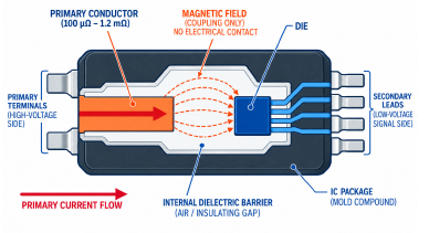
Figure 1: Internal construction of an isolated integrated current sensor, showing magnetic coupling across the dielectric barrier between the high-voltage primary conductor and the low-voltage sensing die and signal leads, with no direct electrical connection between the primary and secondary sides.
As current passes through this primary loop, it generates a localized magnetic field proportional to the current flow. This magnetic field easily penetrates the internal insulation barrier to reach the sensing elements (the Hall plates or TMR stack), which convert the magnetic flux density into a proportional, highly accurate analog or digital voltage output. Because there is no electrical (DC) path between the high voltage primary conductor and the low-voltage secondary circuitry, native galvanic isolation is achieved.
Depending on the package family, this internal separation is realized through one of two die-attach constructions. In wire-bonded packages, the low-voltage sensor die is mounted on the secondary leadframe and connected to its pins by fine bond wires, while the primary conductor is routed as a separate, physically isolated copper leadframe segment beneath or alongside the die. In flip-chip packages, the die is inverted and reflow-soldered directly onto the secondary leadframe via an array of solder balls, eliminating bond wires while preserving the same isolated primary-conductor path. Regardless of which construction a given package uses, the primary and secondary conductive systems never share a direct electrical connection, only the magnetic field generated by the primary current crosses the dielectric barrier to reach the sensing element.
This document is part of a comprehensive series that provides guidance on current sensor selection to help engineers navigate the critical tradeoffs between sensor technologies. For additional content in this series, refer to Beyond the Datasheet: Mastering Current Sensing Selection.
The Fundamentals of Galvanic Isolation in Hall-Effect and TMR Sensors
To appreciate how integrated current sensors achieve robust galvanic isolation, it is necessary to examine the physical architecture inside the plastic mold compound. Unlike traditional current shunts that require a direct electrical connection to a high-voltage line, these sensors achieve separation by maintaining a distinct physical and electrical gap (the internal dielectric barrier) between the current-carrying leadframe and the low-voltage silicon die. This internal dielectric gap forms a high-impedance path that completely blocks direct current (DC) conduction. Instead of an electrical connection, signal transmission is accomplished entirely through magnetic coupling. As the current to be monitored flows through the low-resistance primary copper loop inside the package, it generates a localized magnetic field proportional to the current’s magnitude and direction. This magnetic field seamlessly passes through the internal dielectric insulation barrier to reach the sensitive magnetic transducers on the low-voltage side.
Depending on the specific product selected, the magnetic sensing element utilizes either Hall-effect or Tunnel Magnetoresistance (TMR) technology to read this magnetic field. Traditional Hall-effect sensors utilize integrated silicon Hall plates that generate a voltage proportional to the perpendicular magnetic flux density.
For applications requiring ultra-high bandwidth, lower noise, and superior resolution, patented XtremeSense TMR technology utilizes a magnetic spin-valve stack. This TMR sensor die measures magnetic field angles rather than just perpendicular flux: as the field rotates, it alters the alignment of a magnetic “free layer” relative to a “pinned reference layer” separated by a microscopic magnesium oxide barrier, which modulates the electrical resistance of the stack via quantum mechanical tunneling.
Regardless of whether Hall or TMR technology is deployed, this non-contacting magnetic coupling ensures that no high voltage transients can physically jump to the low-voltage controller circuitry. Furthermore, to combat high-frequency capacitive noise coupling caused by the rapid switching of modern wide-bandgap (SiC and GaN) transistors, dedicated electrostatic shields are integrated directly over the sensor die. These shields provide a low-impedance path that diverts common-mode transient currents to ground before they can couple into the sensitive Hall or TMR signal path. Because this shielding is electrostatic rather than magnetic, it blocks high-frequency electric-field noise without attenuating the magnetic flux the sensor needs to read, preserving signal integrity and preventing false overcurrent faults. Figure 2 and Figure 3 illustrate the fundamental sensing mechanisms of Hall-effect and TMR current sensors, highlighting how each technology responds to an applied magnetic field.
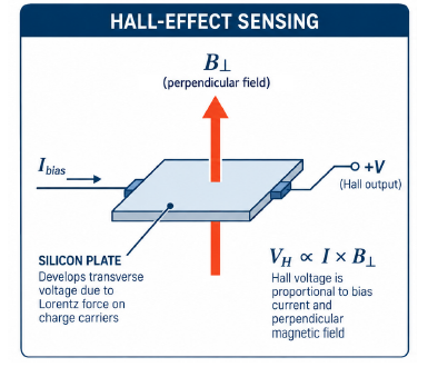
Figure 2: Hall-effect sensing principle: a Hall element responds to magnetic flux density perpendicular to the sensing plane, producing an output voltage proportional to the applied magnetic field.
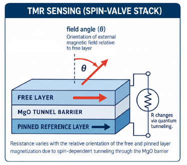
Figure 3: TMR sensing principle: a TMR element detects magnetic-field orientation through changes in resistance within a magnetic tunnel junction, where electron tunneling occurs across the MgO barrier.
Why is Isolation Critical in Application?
Personnel and User Safety
This is the primary reason for isolation. In any system with dangerous voltages, a failure of the isolation barrier could create a direct path from the high-voltage bus to the low-voltage side of the system. This could energize user-accessible parts, such as a metal chassis or communication ports, creating a lethal risk of electric shock. Certified isolation (i.e., to UL or VDE standards) ensures that the sensor provides a reliable, tested barrier that protects human life.
Protection of Low-Voltage Electronics
Without isolation, the high common-mode voltage would be directly exposed to the input pins of the system’s microcontroller. This would permanently damage the microcontroller and could cascade to other low-voltage components on the board. A properly isolated sensor ensures that the output signal is safely referenced to the microcontroller’s own ground, regardless of the high voltage the sensor is measuring.
Noise Immunity and System Performance
Galvanic isolation is a powerful tool for improving signal integrity. In complex systems, different subsystems can have slightly different ground potentials. If a non-isolated sensor is used to connect two such subsystems, it can create a ground loop, which is an unintended conductive path that allows stray currents to flow. This loop acts as a conductor or antenna, picking up electrical noise and injecting it directly into the measurement signal, corrupting the data.
Galvanic isolation is a powerful tool for improving signal integrity. In complex systems, different subsystems can have slightly different ground potentials. If a non-isolated sensor is used to connect two such subsystems, it can create a ground loop, which is an unintended conductive path that allows stray currents to flow. This loop acts as a conductor or antenna, picking up electrical noise and injecting it directly into the measurement signal, corrupting the data.
This is the same ground-integrity problem discussed in the previous installment's treatment of low-side ground bounce, generalized from a single sensor's return-path placement to any non-isolated connection between subsystems at different ground potentials.
By creating a complete electrical break between the high-power side and the low-power control side, galvanic isolation eliminates these ground loops, resulting in a cleaner, more reliable, and more accurate measurement.
Table 1: Isolation function vs. risk-if-absent
| Isolation Function | Risk if Absent | Governing Concern |
|---|---|---|
| Personnel & User Safety | Hazardous voltages may become accessible to users or service personnel, increasing the risk of electric shock. | Safety standards, insulation coordination, working voltage, creepage/clearance, and basic vs. reinforced isolation requirements |
| Protection of Low-Voltage Electronics | High-voltage transients or faults can propagate into MCU, control, communication, or other low-voltage circuitry, potentially causing damage or loss of control. | Galvanic separation, transient withstand, dielectric strength, surge immunity, and system-level fault containment |
| Noise Immunity & System Performance | Fast switching transients and ground-potential differences can couple into the measurement path, producing errors, false trips, or communication/control disturbances. | CMTI, capacitive coupling, ground-loop elimination, common-mode rejection, and signal integrity |
De-Mystifying Allegro Isolation Ratings
When choosing an Allegro current sensor, design engineers must navigate several distinct isolation ratings defined by international safety standards such as UL 62368-1, UL 1577, and IEC 62368-1. Each rating answers a different question, how much voltage the barrier can survive continuously, how much it can survive briefly during a production test, how much physical separation exists between the high- and low voltage sides, how the barrier behaves under fast voltage transients, and matching a system’s bus voltage (e.g., 400 V or 800 V EV battery packs) to the right combination of these ratings is what ultimately determines whether basic or reinforced insulation is required.
Working Voltage
This is the most important specification for long-term reliability. It defines the maximum continuous voltage that the isolation barrier can safely withstand throughout the lifetime of the device. It is determined by factors like the package material, internal spacing, and compliance with safety standards. For example, a sensor like the ACS37002LMA in a SOIC-16W package offers a reinforced working voltage of 565 VRMS, making it suitable for use in 400 V battery systems.
Dielectric Withstand Voltage
This rating (e.g., 2.4 kVRMS or 4.8 kVRMS) indicates the maximum voltage the isolation barrier can endure for a short duration (typically 60 seconds) without breakdown. It is primarily a production-line test to ensure the integrity of the package isolation and is not intended as a continuous operating voltage.
Basic vs. Reinforced Isolation
Basic Isolation provides a single level of isolation sufficient for basic operator protection from electric shock. Reinforced Isolation is a single insulation system that provides a degree of protection against electric shock equivalent to double insulation (two layers of basic insulation). It is required in applications where a failure of the isolation barrier could expose a user to hazardous voltages. By integrating high-performance, high-voltage isolation directly into the sensor package, Allegro devices eliminate the need for costly and complex external isolation components like optocouplers or voltage dividers, enabling safe, simple, and robust high-side current sensing. Table 2 summarizes this distinction alongside typical use cases.
Table 2: Basic vs. Reinforced Isolation Comparison
| Aspect | Basic Isolation | Reinforced Isolation |
|---|---|---|
| Protection level | Single layer of protection against electric shock | Equivalent to double insulation (two layers of basic protection) |
| Required when | A second, independent protective measure exists elsewhere in the system | Barrier failure could directly expose a user to hazardous voltage |
| Relative creepage/clearance/CTI margin | Lower | Higher |
Comparative Tracking Index And Creepage/Clearance
Working voltage and dielectric withstand voltage describe electrical performance, but the isolation barrier is also a physical object, and two measurements, creepage and clearance, determine how much working voltage a given package can safely support in the first place. Figure 4 illustrates the distinction between clearance, measured through air, and creepage, measured along the insulating surface between the primary and secondary sides of an isolated current-sensor package.
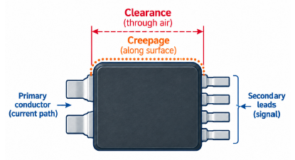
Figure 4: Creepage and clearance paths between the primary current conductor and secondary signal leads of an isolated current-sensor package.
Clearance is the shortest straight-line distance through air between the high-voltage primary leadframe and the low voltage secondary leadframe. Creepage is the shortest path between those same two points measured along the surface of the package’s mold compound. The distinction matters because the two paths fail differently: a clearance gap fails when air ionizes and arcs across it , a fast, voltage-dependent breakdown. A creepage path fails more stealthily, repeated exposure to voltage stress, humidity, and surface contamination can carbonize a track along the mold compound, forming a permanent low-resistance path long before the applied voltage is high enough to break down air alone.
This is why creepage distance requirements are driven by the mold compound’s Comparative Tracking Index (CTI). CTI groups materials by the voltage at which a standardized contaminated-surface test produces tracking failure.
| Material Group | Comparative Tracking Index (CTI) | Creepage Distance | Clearance Distance | Typical Relevance to IC Packages |
|---|---|---|---|---|
| Group I | 600 V | Lowest required creepage for a given working voltage and pollution degree | Not affected by CTI | High tracking-resistant insulating materials |
| Group II | 400 V to 599 V | Higher creepage than Group I | Not affected by CTI | Moderately high tracking resistance |
| Group IIIa | 175 V to 399 V | Higher creepage than Groups I and II | Not affected by CTI | Typical range for many standard IC mold compounds |
In practice, creepage and clearance are set typically by pin pitch and package outline, which is why isolation class tracks package selection so closely. Table 3 summarizes the isolation capabilities for the most common integrated current conductor package families.
Surge and Transient Withstand Performance
Working voltage, dielectric withstand voltage, and surge withstand voltage are often confused because they’re all expressed in volts, but they answer three different questions on three different time scales: Working voltage: what can the barrier survive continuously, for the life of the product? Dielectric withstand voltage: what can the barrier survive for a single, short production test (typically 60 seconds, per UL), before it’s shipped?
Surge (impulse) withstand voltage: what can the barrier survive during a transient event lasting microseconds, such as a lightning-induced surge on an AC line or an automotive load-dump transient, without permanent damage?
Surge withstand is tested with a standardized short-duration impulse waveform (commonly the 1.2/50 µs combination wave defined in IEC 61000-4-5), rather than the sustained AC or DC dielectric test. Some standards combine dielectric withstand testing with partial discharge (PD) testing, applying an elevated AC voltage and measuring for the tiny discharge pulses that indicate a void or defect inside the insulation, since a barrier can pass a simple withstand test yet still contain a latent defect that would fail in the field. Table 4 lines up all four measures against each other for quick reference:
Table 4: Isolation Test Parameter Comparison
| Parameter | Duration | Purpose | Typical Standard |
|---|---|---|---|
| Working voltage | Continuous (product lifetime) | Defines safe long-term operating limit | UL 62368-1 |
| Dielectric withstand voltage | 60 s (one-time, production test) | Screens for gross insulation defects at time of manufacture | UL 62368-1 |
| Surge/impulse withstand voltage | Microseconds (repetitive, transient) | Confirms survival of real-world switching/lightning transients | IEC 61000-4-5 |
| Partial discharge (PD) test | AC, elevated voltage, extended dwell | Detects latent voids/defects for reinforced-isolation certification | NA |
Common-Mode Transient Immunity
Every isolation barrier has some small parasitic capacitance between its primary and secondary sides. When the primary side voltage slews at rate dV/dt during a fast switching edge, that capacitance couples a displacement current across the barrier.
In a system built on fast wide-bandgap SiC or GaN switches, dV/dt can reach tens of kV/µs. If the coupled current is large enough relative to the sensor’s internal bias and reference currents, it can inject noise into the output, or worse, trip a false overcurrent fault at exactly the moment a real fault detection response is needed. This is the same electrostatic shielding mechanism introduced earlier in this note, the shield’s job is to intercept that coupled common-mode current and shunt it to a reference node before it reaches the sensitive Hall or TMR signal path, rather than to block the working magnetic field.
Common-Mode Transient Immunity (CMTI) is specified as a maximum dV/dt (kV/µs) at which the output remains within its accuracy specification with no false trips often depicting the magnitude of the disturbance and the length of time it takes to recover. It’s a meaningfully different spec from working voltage: a sensor can have a very high working voltage (it tolerates a large static common-mode offset) yet a comparatively modest CMTI (it struggles when that offset moves quickly), or vice versa. As discussed in the previous installment of this series, this is exactly why in-line/phase current sensing, where the common-mode voltage swings at the full PWM switching frequency, places the highest CMTI demand of the three topologies. Figure 5 shows what a CMTI-driven false trip actually looks like on the output waveform. A high-CMTI sensor maintains an undisturbed output, while insufficient CMTI can produce a transient glitch that crosses the overcurrent threshold and causes a false trip.
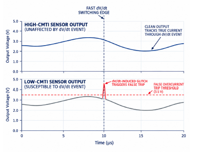
Figure 5: Effect of CMTI on current-sensor output during a fast dV/dt switching transient.
Choosing the Right Isolation Rating: A Decision Framework
Understanding each isolation parameter individually is necessary, but not sufficient. A design engineer still has to move from “Here is my system bus voltage” to “Here is the part number I should evaluate.” The following sequence translates the isolation parameters discussed in this note into a practical device-selection workflow:
- Identify the system’s common-mode voltage. Determine the bus or rail voltage at which the sensor’s high-voltage side will float—for example, 12 V, 48 V, 400 V, or 800 V, as tabulated in the previous installment.
- Determine whether basic or reinforced isolation is required. If a single insulation failure could expose a user-accessible surface—such as a chassis, connector, or enclosure—to hazardous voltage, reinforced isolation is typically required. If a second, independent protective layer already exists elsewhere in the system, basic isolation may be sufficient.
- Select a working-voltage rating with appropriate margin. Do not simply match the sensor’s rated working voltage to the nominal bus voltage. Apply the margin required by the applicable end-system safety standard and expected operating conditions.
- Verify creepage, clearance, and CTI requirements. Confirm that the package geometry and material group satisfy the application’s pollution degree, working voltage, and—where applicable—altitude requirements, rather than relying only on the headline working-voltage rating.
- For SiC or GaN designs, verify CMTI against the expected dV/dt. CMTI must be evaluated independently of working voltage. A device can satisfy the isolation requirements in Steps 1–4 and still experience output disturbances during fast common-mode switching transients if its CMTI is insufficient.
- Confirm the required safety certifications. Verify that the device carries the certifications required by the end application, such as UL 62368-1, UL 1577, IEC 62368-1, or VDE 0884-11. Automotive, industrial, and consumer programs may follow different qualification and certification paths.
Table 5 summarizes these considerations as a quick starting point based on system voltage. For more information on Allegro's packaging options, please refer to our Packaging page.
Table 5: Quick Reference: Isolation Class by System Voltage
| System/Bus Voltage | Typical Isolation Direction | Package Recommendation | Allegro Part Number |
|---|---|---|---|
| 12 V standard automotive | Basic or no galvanic isolation, depending on topology | LH EX |
ACS37041KLH, ACS71240KEX |
| 48 V mild-hybrid/e-bike | Basic | EZ LC |
ACS37220LEZ, ACS37010LLC, ACS71240LLC |
| 400–650 V industrial motor drives | Reinforced | LZ MA/LA MY MZ |
ACS37030LLZ/ ACS37032LLZ ACS37002LMA/ ACS37002LLA ACS37030MY/ ACS37032MY ACS37220MZ |
| 400–800 V EV/HEV traction | Reinforced | MA MY MZ |
ACS37100LMA ACS37030LMY/ ACS37032LMY ACS37220MZ |
| 800–1000 V next-generation SiC/GaN | Reinforced + high CMTI | MA MC |
ACS37100LMA ACS37002LMC |
Conclusion
Galvanic isolation is not a single number on a datasheet; it’s a stack of related but distinct specifications — working voltage, dielectric withstand voltage, surge/impulse withstand, creepage and clearance (governed by the mold compound’s CTI), and common-mode transient immunity — each answering a different question about how the barrier behaves, on a different timescale, under a different kind of stress. As shown throughout this note, Allegro’s Hall-effect and XtremeSense TMR sensors satisfy this entire stack inside the package itself, through physical separation of the primary conductor from the sensing die, rather than through external isolated amplifiers, optocouplers, or isolated bias supplies bolted onto a shunt-based signal chain.
As established in the previous installment of this series, High-Side vs. Low-Side Current Sensing: Why Placement Matters, the decision to place a sensor on the high side or in-line with the load is what makes galvanic isolation mandatory rather than optional. This installment has shown how that mandate is actually satisfied at the package level, and how to translate a system’s voltage and switching environment into a specific isolation class, package, and part number.
Isolation and safety, however, only answer whether a measurement can be safely captured — not how quickly or how accurately it can be captured. Having established how the barrier safely and reliably crosses the voltage domain, the next installment in this series turns to the time domain: *Dynamic Response*, examining how bandwidth, propagation delay, and response time determine whether a safely isolated sensor is also fast enough to protect the system it’s isolating.
| Allegro Package | Package / Form Factor | Minimum Creepage | Minimum Clearance | Basic Isolation | Reinforced Isolation | Example Integrated Current Sensor |
|---|---|---|---|---|---|---|
| SOIC-16 | ||||||
| LA | Wide-body SOIC-16 | 7.5 mm | 7.5 mm | Yes | Yes | ACS37002LLA |
| MA | Wide-body SOIC-16 | 7.9 mm | 7.9 mm | Yes | Yes | ACS37002LMA/ ACS732KMA |
| MC | Custom wide-body SOIC-16 | 8.7 mm | 8.7 mm | Yes | Yes | ACS37003KMC |
| SOIC-8 and Custom Fused-Lead SOIC-6 | ||||||
| LC | Narrow-body SOIC-8 | 4.0 mm | 4.0 mm | Yes | No | ACS71240LLC, ACS37010LLC |
| LZ | 6-pin fused-lead SOIC | 4.1 mm | 4.1 mm | Yes | Yes | ACS37030LLZ/ ACS37032LLZ |
| MY | 6-pin fused-lead wide-body SOIC | 8.5 mm | 8.5 mm | Yes | Yes | ACS37030LMY/ ACS37032LMY |
| MZ | Wide-body SOIC-6 | 8.5 mm | 8.5 mm | Yes | Yes | ACS37220LMZ |
| QFN with wettable flank | ||||||
| EZ | 7-pin 4 × 4 mm QFN | Not specified as safety creepage | Not specified as safety clearance | No - functional only | No | ACS37220LEZ |
| EX | 12-contact, 3 × 3 mm QFN | Not separately specified | Not separately specified | No - functional only | No | ACS71240KEX |
| High-Current Custom Allegro Packages | ||||||
| LX | Compact PSOF-8 | 8.0 mm | 8.0 mm | Yes | Yes | ACS37200LLX |
| CB | Custom high-current 5-pin package | 6.9–7.25 mm | 6.9–7.25 mm | Yes | Yes | ACS772CB, ACS773CB |
| Compact SOT23-W | ||||||
| LH | Compact SOT23-W | 2.0 mm | 1.9 mm | Yes (ACS37042 only) | No | ACS37041LLH/ ACS37042LLH |
This document is part of a comprehensive series that provides guidance about current sensor selection. For additional content in this series, refer to Beyond the Datasheet: Mastering Current Sensing Selection.