Have Questions? Let us help!
We're passionate about innovation. Reach out and you'll hear back from an expert shortly.
One of our solution experts will be in touch with you shortly. Keep reading to learn more about our industry leading solutions.
Table 1. ACS710-12C Noise Level and Current Resolution | ||||
CF | BW | VRMS Noise | VP-P Noise | Current Resolution |
0 | 120 | 1523 | 9138 | 163 |
1 | 94 | 1185 | 7110 | 127 |
2.2 | 43 | 1010 | 6060 | 108 |
4.7 | 20 | 874 | 5244 | 94 |
10 | 9 | 768 | 4608 | 82 |
22 | 4 | 724 | 4344 | 78 |
47 | 2 | 682 | 4092 | 73 |
Table 2. ACS710-25C Noise Level and Current Resolution | ||||
CF | BW | VRMS Noise | VP-P Noise | Current Resolution |
0 | 120 | 994 | 5964 | 213 |
1 | 94 | 948 | 5688 | 203 |
2.2 | 43 | 713 | 4278 | 153 |
4.7 | 20 | 658 | 3948 | 141 |
10 | 9 | 602 | 3612 | 129 |
22 | 4 | 570 | 3420 | 122 |
47 | 2 | 536 | 3216 | 115 |
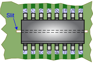
The creepage distance on the surface of the sensor IC package measures approximately: 7.50 + 2.00 = 9.50 (mm)
The creepage distance on the surface of the printed circuit board on which the sensor IC is mounted may be increased, if necessary, by cutting a slit on the board between the solder pads on opposite sides of the sensor IC package. Refer to figure 4.
|
Table 3. ACS710-12C Input Current versus Power-On Time |
|
|
IP |
tPO |
|
0 |
14 |
|
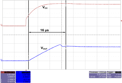
12.5 |
16 |

|
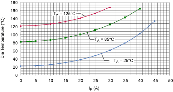
Table 4. Continuous Current Overcurrent Limits |
|
|
tA |
IP(OClim) |
|
25 |
45 |
|
85 |
35 |
|
125 |
25 |
|
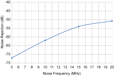
Table 6. Typical Capacitive Coupling of |
||
|
Frequency |
VOUT |
Noise Rejection |
|
5 |
5 |
−72 |
|
10 |
16 |
−62 |
|
15 |
40 |
−54 |
|
20 |
58 |
−51 |