Single Gate Driver Design Enables Wide Range of Battery Voltages for Various Motor Power Levels
When designing a product portfolio with a wide range of voltage and power requirements, finding a single driver design solution to serve the full portfolio can deliver significant savings in time and resources. Designs that are capable of handling a wide range of battery voltages require high-efficiency operation with the capability to drive a wide range of MOSFET gate current and voltages, accommodate high thermal dissipation, and withstand very large negative transients. This article discusses these challenges when trying to accommodate wide-ranging battery voltages and motor powers in a single driver design and highlights a commercially available solution that can help designers achieve this goal.
To drive motors or drivers for high-voltage, high-power applications where low noise with high efficiency is the critical design factor, the continuing design trend is to use permanent magnetic synchronous motor (PMSM) drives and/or brushless DC (BLDC) drives. For many other applications, such as those where the acoustic noise of the mechanical processing usually drowns out the motor noise, simple DC motors that can be driven with a simple half-bridge architecture are still adequate. Nevertheless, running a motor/driver with a wide power range causes power dissipation and switching effects that pose significant challenges for both three-phase drives and DC drives, so the considerations here are valid for either.
High-Voltage and High-Power DC Motor Operation
Running a DC motor may seem like a simple task. However, it still presents challenges, including the need to sustain high-voltage operation to support dissipation of motor inductance energy when braking. To address this challenge in applications where the driver stage must be suitable for use with a wide power range, designers require solutions that enable both high-voltage operation and the capability to handle huge negative transients.
A wide-ranging power solution also requires the capability to drive a wide range of gate currents for medium-power to high-power MOSFETs, which introduces high power dissipation inside the device. To address this power dissipation, designers may find the best solutions in drivers with low driving impedances.
Driving a MOSFET requires an understanding of the MOSFET switch waveform, discussed next.
Understanding MOSFET Switching Behavior
For inductive loads like motors, the switching cycle can be divided into four phases:
- t0 to t1 → Gate voltage rises to the threshold voltage.
- t1 to t2 → Drain current (iD) rises, and gate voltage rises according to the transconductance of the MOSFET.
- t2 to t3 → Drain-to-source voltage (VDS), falls [not linear because input capacitance (CISS), output capacitance (COSS), and reverse transfer capacitance (CRSS) are dependent on (VDS)] and the gate current charges the Miller capacitance (VGS), during which time, (VGS) is stable.
- t3 to t4 → VDS is saturated low, and VGS rises to it's final value.
These phases are illustrated in Figure 2.
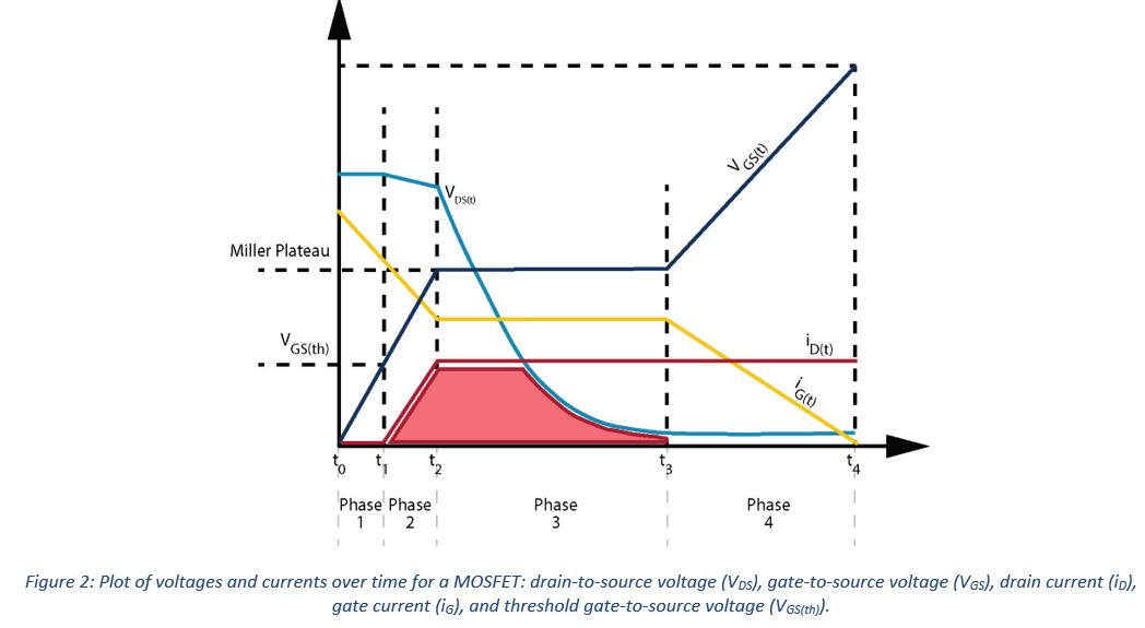
The gate-to-source voltage at the start of Phase 1 (VGS(t)) is zero, and the flow of the gate-drive current (iG(t)) that the driver needs to supply is at its peak. This maximum drive strength is not needed for the total switching time (t0 to t4) because the gate capacity becomes successively charged.
Approximately, the typical turn-on time can be obtained by:

where:

In general, to keep the power budget low, fast switching is desired. On the other hand, in most cases, gate drive current needs to be limited to control switching speed (i.e., dV/dt) to meet electromagnetic compatibility (EMC) requirements. By adding a gate resistor (RGATE), turn-on time can be extended according to:

Several effects need to be weighed when increasing the gate resistor. Increasing the gate resistor will:
- Increase the switching losses (i.e., increase the light red area in Figure 2).
- Decrease the demand for driving power from the gate driver. This effect is generally desirable because it results in less power dissipation from the driver itself, so less heat is produced. The tradeoff is a longer time to charge the total gate capacitance of the MOSFET and an increase in the power dissipated on the gate resistor (i.e., a higher voltage drop occurs for a longer time). In other words, the power losses shift from the driver to the gate resistor.
- Increase the dead time.
The best tradeoff needs to be found to account for all of these effects.
Understanding MOSFET Fast-Switching and the Miller Effect
In addition to the MOSFET switching behaviors and tradeoffs discussed above, fast switching can cause another appearance of the known Miller effect, which must be considered in a design. The Miller effect can lead to an induced VGS bounce caused by a gate inrush current, according to:
IG = CGD × dVDS/dt.
The name stems from the gate-to-drain capacity of a MOSFET, also termed the Miller capacity.
To illustrate the Miller effect, all MOSFET capacities in a half bridge are shown in Figure 3. The input capacitance (CISS), output capacitance (COSS), and reverse transfer capacitance (CRSS)—values that are typically indicated in the MOSFET datasheet—are related to the gate-to-drain capacitance (CGS), gate-to-source capacitance (CGS), and drain-to-source capacitance (CDS) as follows:
CISS = CGD + CGS
COSS = CDS + CGD
CRSS = CGD
These relations can be rewritten as:
CGD = CRSS (CGD = Miller capacitance)
CGS = CISS – CRSS
CDS = COSS – CRSS
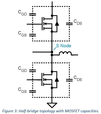
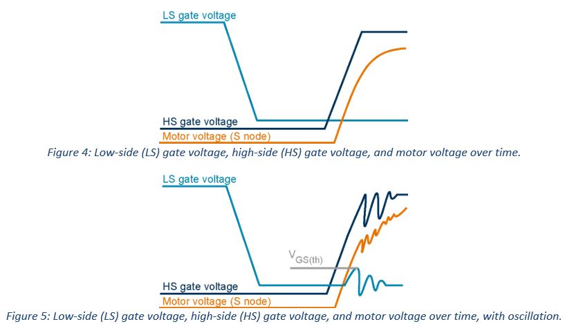
An example of ideal gate drive signals of both the high side and the low side with sufficient dead time and with motor voltage monitored at the S node is shown in Figure 4. In contrast to this ideal, the high-side and low-side gate voltages might be observed in practice as shown in Figure 5. The difference between the ideal and the actual is explained by the switching behavior. When switching-on the high-side gate, the fast dV/dt transient of the S node causes the low-side gate voltage Miller capacitance (CGD) to recharge, pulling the VGS of the low-side MOSFET above the low-side gate threshold voltage (VGS(th)). This leads to cross-conduction resulting in oscillation at the S node and extensive power losses. Reducing the low-side MOSFET gate resistor in contrast to the high-side MOSFET gate resistor and using an adequate snubber on the S node can mitigate this effect. Significant improvements can be reached by adding an additional ceramic capacitor in parallel to the high-side gate capacitance, which would reduce dV/dt.
Leveraging MOSFET Capacities to Avoid the Miller Effect
A method to avoid the Miller effect can be understood using the Allegro APEK89500 demonstration board designed to evaluate the Allegro A89500.
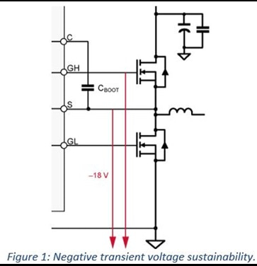
The A89500 is ideal for this illustration. It is a fast-switching half-bridge MOSFET driver designed to enable both high-voltage operation [e.g., high side and low side: 2.7 A source current (typical) and 5.2 A sink current (typical)], with scaling up to a 100 V bridge supply and to handle up to –18 V transients at the high-side gate output terminal and the high-side source (load) terminal, such as illustrated in Figure 1. For a dual-flat no-leads (DFN) package, the A89500 has a very low package thermal-resistance junction to ambient (RƟJA)—38°C/W for a two-layer 3.8-inch × 3.8-inch PCB (for additional information, see the A89500 datasheet). of the switching cycle, the approximation used in this article for the charging time of a capacitor connected directly to the driver is also used in the datasheet (see excerpt, 4 to t0To assist designers in understanding the maximum drive strength the driver needs to supply throughout all phases tTable 1).

The APEK89500 demonstration board designed to evaluate the A89500 can demonstrate the capability of the A89500 to avoid the Miller effect and deliver low-noise, high-efficiency operation. The board deploys two MOSFETs with the capacitances shown in Table 2.
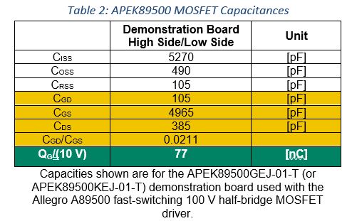
The APEK89500 demonstration board was setup without optimization for a reference design for the design target. This deliberate lack of optimization resulted in susceptibility to the Miller effect. Despite the lack of a reference design for the design target, the Miller effect could be completely canceled out by adding a 1 nF capacitor in parallel to the high-side gate capacitance CGS. The reduction of the CGD/CGS ratio is shown in Table 3. When implementing designs that use the A89500, a good approach that completely avoids the Miller effect is to maintain a similar reduction ratio.
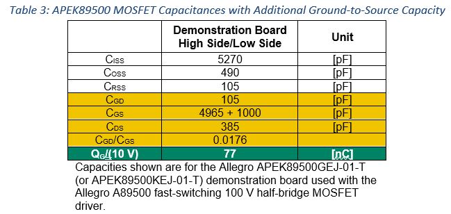
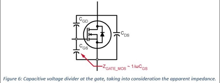
As shown, adding a capacitor in parallel to the high-side gate capacitance CGS will cause a reduction in dV/dt at the S node and will therefore mitigate the Miller Effect. This result can also be leveraged by reducing the CGD/CGS ratio at the low side as well (e.g., by adding a capacitor parallel to the low-side gate capacitance). This approach becomes comprehensive when considering CGD and CGS as a voltage divider (see Figure 6). Thus, when increasing CGS, the apparent gate-to-source impedance becomes smaller, which further supports the effort to keep the gate well below VGS(th).
Of course, a proper CGD/CGS ratio can be obtained by using a MOSFET that is appropriate for the design. Additional measures to avoid a capacitive switch on the low side include using a low-side MOSFET gate resistor that is reduced in contrast to the high-side MOSFET gate resistor and a snubber on the S node to mitigate the effect of cross-conduction (Allegro representatives are available to provide support).
Finding One Driver Solution for Wide Voltage and Power Requirements
When designing a product portfolio with a wide range of voltage and power requirements, the A89500 from Allegro MicroSystems is a simple and robust driver solution. This 100 V high-power half-bridge gate driver in an ultra-compact DFN package allows fast switching with low switching losses when good design practices are followed. The A89500 is a solution that can accommodate high thermal dissipation, withstand very large negative transients, and support phased voltage changes, which are needed to drive a wide range of MOSFET gate currents and voltages.
Based on the article, "How gate driver enables a wide range of battery voltages" by Christian Huber, originally published in Electronic Design News, February 8th, 2023. Republished with permission. For portions not copyrighted by original publisher, Copyright ©2023, Allegro MicroSystems, Inc.
Copyright 2022, Allegro MicroSystems.
The information contained in this document does not constitute any representation, warranty, assurance, guaranty, or inducement by Allegro to the customer with respect to the subject matter of this document. The information being provided does not guarantee that a process based on this information will be reliable, or that Allegro has explored all of the possible failure modes. It is the customer’s responsibility to do sufficient qualification testing of the final product to ensure that it is reliable and meets all design requirements.
Copies of this document are considered uncontrolled documents.