Pre-Emptive Boost Control Improves LED Driver Performance
Recent advances in the area of pulse-width modulated (PWM) dimming control of have dramatically increased the maximum achievable dimming ratio, reduced output voltage ripple, and eliminated audible noise. This article describes a new family of LED drivers that employ a patented pre-emptive boost (PEB) control algorithm to reduce output voltage ripple when using PWM control for LED dimming. It demonstrates the PWM dimming benefits achieved by PEB when compared to the behavior of conventional LED driver control methods.
PWM control is commonly used for LED dimming by controlling the average current through one or multiple LED strings. This is accomplished by varying the duty-cycle of a control pulse at an input to the LED driver device.
Allegro MicroSystems’ automotive AEC-Q100 qualified A8060x / ALT8060x family (or A8060x hereafter unless specified), the company’s latest generation of advanced LED backlight drivers, uses Pre-Emptive Boost control to offer distinct advantages over conventional boost control methods for PWM dimming of LEDs.
Advantages of PEB control over traditional and hysteresis control include:
- Lower output voltage ripple allows the use of smaller output capacitors, reducing solution size and cost.
- Lower output voltage ripple also eliminates audible noise in ceramic output capacitors.
- It allows greater PWM dimming ratios (smaller pulse widths) while remaining in regulation.
PWM CONTROL METHODS
Traditional Boost Control
When the PWM control signal changes logical state, a traditional boost control LED driver turns its boost switching and LED current sinks on or off simultaneously. After a positive-going PWM signal transition, it takes multiple switching cycles for the inductor current to ramp up to its steady-state value. During this time, LED current is primarily drawn from the output capacitor. This draw causes the output voltage to droop and can result in audible noise from the MLCC output capacitor and substantial output voltage ripple.
In addition, this output voltage droop limits how short the PWM signal on-time can be because the output needs adequate time to recover. On-times that are too short will not provide adequate time for the boost converter to replenish the energy in the output capacitor, resulting in output voltage dropout and LED current regulation lost. This severely limits the PWM dimming ratio that can be achieved.
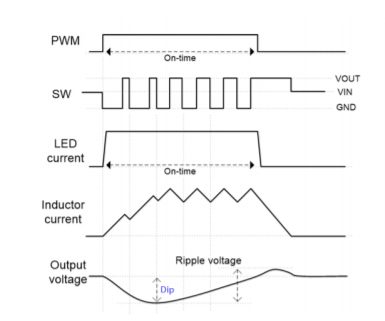
Figure 1: Traditional PWM dimming operation. Boost switch and LED current sinks are enabled and disabled at the same time.
Hysteresis Control/Boost Extension
An improvement to the traditional boost control described above is to extend the boost switching for a period after the LED current sinks turn off, effectively pumping up the output voltage slightly past the normal regulation voltage. This is achieved by implementing a hysteretic control loop that increases the Vout regulation voltage by a determined amount whenever Vout drops below a certain voltage. This hysteresis (boost extension) control allows operation with a shorter PWM signal on-time than traditional boost control, resulting in a larger achievable dimming ratio, but still a smaller ratio than is achievable with preemptive boost control. Similar to traditional boost control, the hysteresis control method exhibits large output voltage dips at the start of boost switching that can result in large output voltage ripple and audible noise.
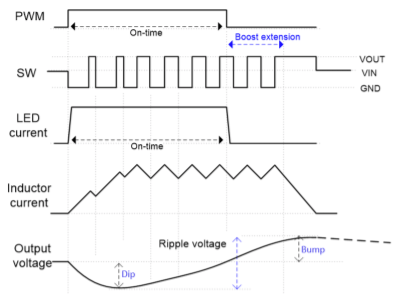
Figure 2: Hysteresis control PWM dimming operation. Boost switch and LED current sinks are enabled simultaneously,
but boost switch remains enabled for a time to pump up Vout.
Pre-Emptive Boost Control
Allegro MicroSystems’ patented pre-emptive boost control (PEB) provides a solution that results in substantially reduced output voltage ripple. PEB also allows operation with a smaller PWM signal on-time, allowing PWM dimming ratios of up to 15,000:1.
PEB control works by delaying the startup of the LED current sinks with respect to the start of boost switching. This allows time for the average inductor current to increase before the current sinks turn on and demand current. The result is an initial slight increase in output voltage; however, the pre-boosted inductor current results in negligible output voltage droop when the current sinks turn on.
In order to maintain accurate PWM control, an identical PEB delay is imposed after the PWM control signal transitions low. With this control method, both boost switching and the current sinks turn off at the same time.
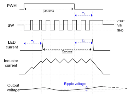
Figure 3: Pre-emptive boost control PWM dimming operation. LED current sinks remain off until the inductor current is sufficient to prevent VOUT droop.
CALCULATING AND OPTIMIZING PRE-EMPTIVE BOOST DELAY
When calculating pre-emptive boost delay, multiple factors affect the optimal pre-emptive boost delay time (tPEB). These factors include, but are not limited to: Vin, Vout, switching frequency, inductor value, and LED current. The following equation can be used to approximate the tPEB setpoint:

where fs is the switching frequency, and L is the inductance of the boost inductor.
It is ideal to set tPEB so that the LED current sinks turn on at the point when the average steady-state inductor current is reached. tPEB is set by a resistor from the PEB pin of the A8060x to ground. Once tPEB is approximated, the PEB delay vs. PEB resistor value curve in the pre-emptive boost section of the A8060x’s respective datasheet should be used to determine the resistor value.
Equation 1 can be used as a starting point, but it is an approximation, and not all factors that affect the behavior are taken into account. While even non-optimized PEB delay time can significantly improve the output voltage ripple, it is preferable to optimize this delay with some fine-tuning in the laboratory. The following example application demonstrates the results of this optimization.
Example Application
The following application will be evaluated and optimized for Vout ripple:
- LED driver with 6 strings of 8 LEDs each.
- Nominal Vin: 13.5 V.
- Vout: 26.5 V.
- Output current: 6 strings at 100 mA/string when current sinks are active.
- Boost inductor: 10 μH.
- Switching frequency: 2 MHz.
- LED driver used: Allegro MicroSystems A80602.
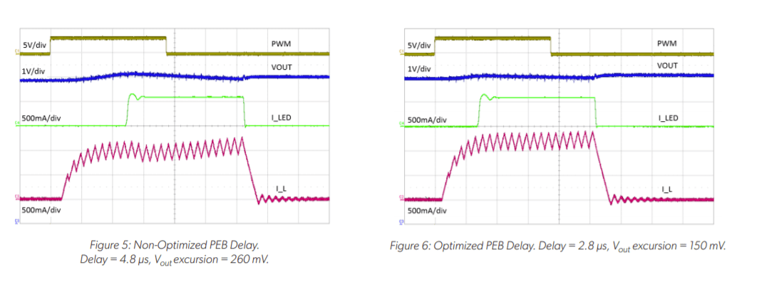
Entering Vin, Vout, boost inductor value, and switching frequency into Equation 1 yields an initial tPEB set point of 4.8 μs. Referring to Figure 4, it is determined that a value of 9.6 kΩ from the PEB pin of the A80602 to ground will result in a delay of about 4.8 μs.
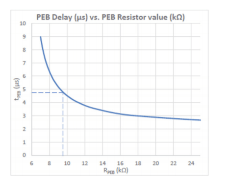
Figure 4: A80602 PEB Delay. Resistor Value vs. Delay Time.
Optimizing Pre-Emptive Boost Delay
After calculating the approximate PEB delay, the final step is to build and evaluate it in the lab. At this point, tPEB can be optimized to minimize Vout ripple. Figures 5 and 6 show the non-optimized and the optimized PEB delay, respectively. While the longer non-optimized delay results in very satisfactory Vout ripple performance, this ripple can be further reduced by adjusting tPEB so that the LED current sinks turn on as soon as the average inductor current is reached. In this example, the optimization reduced the Vout overshoot from 260 mV to 150 mV.
PEB CONTROL REDUCES OUTPUT CAPACITOR REQUIREMENTS
The Pre-Emptive Boost control results in a substantially smaller output voltage ripple than traditional or hysteresis boost control. As a result, far less output capacitance is needed, leading to reduced solution size and cost. Figure 7 shows a comparison of a hysteresis boost control LED driver and one with PEB control. Three different Vout traces are shown. The top trace is Vout of the hysteresis boost control LED driver. The next trace shows Vout of the PEB control LED driver with the same output capacitance as the hysteresis boost control device. The third trace is Vout of the same PEB control device, but with only 25% of the output capacitance. Even with this drastically reduced output capacitance, the converter with PEB control exhibits a smaller output voltage ripple than the converter with hysteresis boost control.
When PWM transitions high, with PEB control, Vout does not overshoot significantly. However, when PWM is low, the converter is not regulating and Vout droops. This droop is dependent upon output capacitance, PWM frequency, and PWM duty cycle. For a given PWM frequency and duty cycle, a greater output capacitance will reduce Vout droop, and in turn, reduce total Vout ripple. The effects of reducing the output capacitance can be seen when comparing the two lower Vout traces in Figure 7.
Audible noise generated by ceramic output capacitors is common in applications with a high Vout ripple. As the capacitor case size is increased, this noise tends to become worse. A decrease in the necessary output capacitance allows the use of smaller case size capacitors, reducing audible noise levels. The large Vout ripple, as is demonstrated with the hysteresis boost control trace in Figure 7, can result in audible noise in some applications. The reduced Vout ripple that results from PEB control solves this issue.
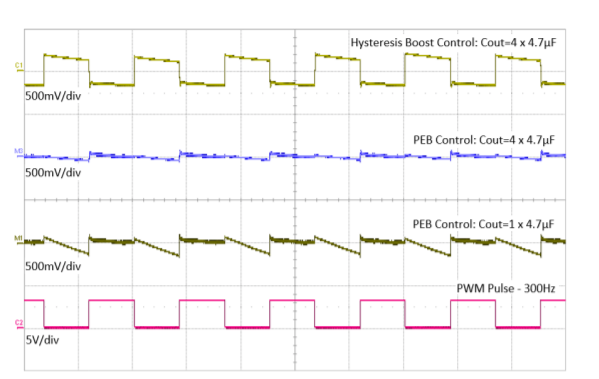
Figure 7: Vout Ripple, Hysteresis Control vs. PEB Control.
OTHER FEATURES
The A8060x family is a versatile, feature-rich family of LED drivers that are ideally suited for automotive applications such as infotainment backlighting, head-up displays, and interior/exterior lighting. They are automotive AEC-Q100 qualified, offer extensive fault protection features, and have a wide input voltage range to meet load dump, stop/start, and cold crank requirements.
The ALT80600 and A80603 combine a switching converter with an integrated boost MOSFET, while the A80601, A80602, A80604, A80605, A80606 drive an external boost MOSFET for greater output power. The ALT80600, A80601, A80603, and A80604 have four LED current sinks, while the A80602, A80605, and A80606 have six current sinks. Some or all of these current sinks may be connected in parallel for higher current applications. Each of these devices can be configured in a boost or single-ended primary-inductor converter (SEPIC) topology to cover a wide range of application configurations. The switching converters are designed for low EMI, offering features including programmable switching frequency, controlled switching slew rate, and programmable dithering.
The A8060x family’s pre-emptive boost control allows for a substantial PWM dimming ratio of up to 15,000:1. If further dimming is desired, the A8060x’s analog dimming feature can be used to increase the maximum dimming ratio to 150,000:1.
To learn more about the A8060x family and ALT80600 visit www.allegromicro.com/led-drivers-for-backlighting
Originally published in Elektronik Industrie, October 2019, pp. 38-41. The original article and full publication can be found here. Republished with permission. For portions not copyrighted by original publisher, Copyright ©2021, Allegro MicroSystems, Inc.
-
Download Original PDF [German]