
使用动态正交偏移消除的单片磁性霍尔传感器 IC
作者:Alberto Bilotti(IEEE 终生高级会员)、Gerardo Monreal 和 Ravi Vig
摘要—偏移电压及其温度漂移和生产偏差通常会降低磁霍尔传感器 IC 的零电平稳定性和重现性,通过使用用于电源和输出触点对的周期性换向的单个霍尔板和切换方法,可以减少这些偏移、漂移和偏差。本工作描述了斩波型 5-V 单片线性霍尔传感器 IC(带有 ±0.1 T 满量程),在该传感器 IC 中已经采用了这项动态板偏移消除技术以及具有成本效益的信号调节器。此设备使用 2-µm 传统 BiCMOS 工艺集成,尺寸为 1.5 × 1.5 mm 的最终芯片采用 3 引脚塑料封装,具有带有生产偏差的残余偏移,其温度漂移仅为目前多板直流正交消除方法产生漂移的五到十分之一。此设备不需要外部组件,可提供无高频残留的输出。
索引术语—BiCMOS 模拟集成电路、斩波器、霍尔效应器件/效应、微型传感器、单片集成电路。
I. 简介
单片磁传感器 IC 通常使用硅霍尔效应元件,这些元件可轻松集成放大器或信号调节器电路,以进行放大,或处理生成的相对较低电压。霍尔效应、该器件特性以及应用等内容已经在文献 [1]−[3] 中进行了广泛的研究讨论。Baltes 和 Popovic 的文章提供很多带参考文献的精彩评论。
最简单的霍尔效应元件使用方形板,例如,采用双极或者 BiCMOS 工艺的 Epi-pocket(带有两对正交触点),如图 1 所示。将电源电压 Vs 加到一对触点(如 a、c),垂直于方形板的磁感应强度B在另一对触点 b、d 上产生电压 VH,
其中 Sv 表示单位电源电压的霍尔效应元件灵敏度。VH ⁄B × Vs[T-1] 给定灵敏度,其中 T(特斯拉;1 T = 1 × 10⁴高斯) 是磁通密度(感应)的米-千克-秒 (mks) 制单位,它大致是一个常量参数,仅取决于硅层迁移率以及方形板和触点的几何形状。Sv 值通常在 0.04 到 0.08 T-1 之间,这意味着,对于典型的 5 V 电源和最低磁通密度 1 mT,输出电压在 200 到 400 µV 之间。
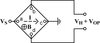
图 1.基本霍尔板。
在所有直流应用中,霍尔板能够精确测量的最低磁通密度取决于B= 0 时,霍尔板输出触点上出现的偏移电压 Vop。从电气的角度来看,霍尔板将因电阻梯度、几何不对称 [4]、压阻效应 [5],[6]等因素产生不可忽视的偏移电压。由于霍尔板偏移量 Vop 较大—,对于 5-V 电源,其偏移范围可能为 0.5 到 5 mV,并且会受温度、供电电压和应力的影响,—技术人员一直为消除或或尽量减少其影响而努力。
放大器使用的开关技术无法消除偏移,这是因为不存在能将 Vop 与 VH 分离的可用状态,除非切断磁场,这当然是行不通的。
注意,从直流的角度来看,霍尔板可被视为分布电阻式惠斯登电桥,目前大多数商用霍尔传感器 IC 通过使用两个或者更多适当互连的霍尔板来消除偏移,其中一个霍尔板的电流方向与另一个霍尔板的电流方向之间的夹角为 90°[7]。如果空间存在固定不变的不平衡源,则任何成对霍尔板的偏移量将大小相等、方向相反,从而实现所需的偏移消除。另一方面,多板排列的有用信号仍然和单板的相等。
另外,有人还提出仅使用一块板,通过电源和输出触点的周期置换来生成正交状态 [8],[9]。虽然这项动态偏移消除技术需要在霍尔开关板后使用更复杂的信号调节器,但它有一个优点:与多板传感器 IC 相比,它可以减少残余偏移和生产偏差。对于后者,由于存在物理差别的各板之间的板偏移不匹配,零电平偏移发生退化,这些不匹配主要是受塑料封装温度影响的内置应力所致。
本文描述了使用动态偏移消除技术的 5 V BiCMOS 单片线性霍尔传感器 IC,这项技术通过具有成本效益的信号调节器来执行各种必需的功能,以恢复有用信号并消除偏移。
为获得简单的高增益开环放大器,应首选 BiCMOS 工艺。此放大器的偏移小,具有精确的温度设定电路和低成本、高输出电流源功能。
II.开关型霍尔板
最简单的动态偏移取消技术使用带四个触点的方形板,通过以周期方式将电源电压和电源调节器输入连接到一对触点或者另一对触点,来生成正交状态,如图 2 所示。从现在开始,我们要将每个状态称为 0° 状态或90°状态,并由互补时钟 CLK1 和CLK1_bar 分别定义。
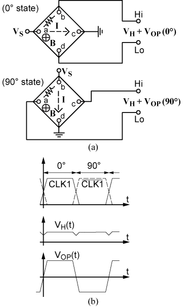
图 2。(a) 在动态偏移取消技术中,流过方形板的电流被定期从 0° 切换到 90°方向,反之亦然。(b) 时钟、霍尔电压和板偏移量波形。
假设 B= 0 且霍尔板采用理想的惠斯通电桥模型,则输出触点上的电压为板偏移量 Vop(0°) 和Vop(90°),它们大小相等,但是极性相反。这一点可通过下面所示的一种非常简单的方式验证。假设因应力模式导致失衡,使得触点 a 和 b 之间的电阻率小于霍尔板的其他位置(图 2 中的虚线电阻器),且在更改状态时,这种情况不会改变。然后,在每个状态形成的偏移具有同样的幅值,但是极性相反,这是因为在等效电桥网络的相邻支路发生了同样的不平衡(在 0 °状态 Hi 端子的电压将高于 Lo 端子,在 90°状态 Hi 端子的电压将低于 Lo 端子)。
对于 B ≠0,由于电源和输出连接旋转方向相同,VH 保持其极性不变,这使 VH 不变。VH 的这一特性源于对称霍尔板的反可逆属性。
因此,就出现了一种可以将偏移与有用信号区分开来的方法,通过适当的信号调制还可以进一步消除偏移。虽然图 2 中 VH是准恒定值,Vop 是交替方波,但如果需要,可通过在 90° 状态下将输出触点 a 和c 互换来实现波形互换。
由于无法实现理想情况下的完全消除,在实践中将残余板偏移 Vop (r) 定义为
其中,首选使用绝对值,以强调在进一步信号处理期间发生的极性逆转。根据制作工艺、霍尔板几何形状和结晶方向,以及残余晶片和封装应力的情况,对于 5 V 电源,Vop(r)可能介于 50 到 500 µV 之间。
在单板上,无论是 Epi 板 [9] 还是 MOS 通道“板”[10],与传统多板方法相比,正交消除的直流测量数据都显示出比较明显的改善。为减少 Vop(r),在“旋转”霍尔元件中,使用在圆板边缘分布的四对触点来执行这些测量[9]。在这种情况下,用于改进偏移消除效果的所有可能偏移的多路增加,需要每个周期有八个开关状态。
为了简化和减少芯片面积,为我们的单片传感器 IC 选择最简单的 Epi 板,此板配有两对触点,每个周期两相,如图 2 所示。
最大允许开关频率取决于每次换向转换后的板电压稳定时间。请注意,例如,在 0° 状态转换到 90°状态后,在图 2 中触点 a 的电压Va将从Vs降至Vs ⁄ 2,而 Vc 将从零增加到 Vs ⁄ 2 (d 和b 处的电压将分别衰减到地电位和增加到Vs)。这要求对在 Epi-Sub 反向偏置结点存储的电荷进行重新排列,因此,经过一定的时间后,电压稳定至最终电压 Vs ⁄ 2。之后,霍尔输出电压将变为有效电压并接受处理,如图 3 所示。
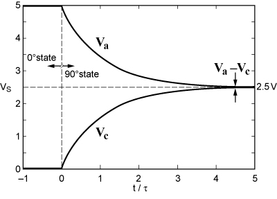
图 3。0° 状态到 90° 状态霍尔板开关瞬态,其中 Va 和 Vc 分别是图 2 中触点 a 和触点 c 的电压。
对在 2 Ω-cm、5.5 µm 厚的方形 Epi 层上构建的霍尔板(对角线触点之间的电阻为 3 kΩ)进行的开关测量表明,霍尔电压在板换向转换完成 ≈600 ns 之后才会生效。考虑到组件公差,以及每相必须包含其他示例脉冲,从而得出霍尔板的最大开关频率为 200 kHz。只要开关频率仍然低于此限值,开关频率就不是系统工作的关键因素,简单讲就是时钟回路执行。
即使稳定时间过长导致存在残余电压,此电压在两种状态下都会保持不变,正如真实偏移一样,因此将被抵消。由于需要非常精确并且更昂贵的 CLK 发生器,因此没有对此问题进行深入研究。
图 4 显示了在单片传感器 IC 中使用的实际开关板排列布置,其中触点换向所需的四个单刀双掷 (SPDT) 开关是利用 MOS 晶体管实现的。板触点互连遵循图 2 的基本方案,只是在 90 ° 状态下输出端子应互换。利用此布置方案,每次更改状态时,VH 改变极性,Vop保持准恒定,采用这种方式,VoA、运算放大器 A1 的直流输入参考偏移将无法与 Vop 区分,并且霍尔板偏移和输入放大器偏移将由信号调节器同时处理和消除。
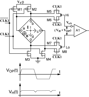
图 4。开关霍尔板。在 CLK1 信号处于高电平时,电流在a 和 c(0°状态)之间流动,当 CLK_bar 信号处于高电平时,电流在 b和 d 之间流动(90°状态)。
这样,无需任何代价即可消除 A1 偏移,从而避免了采用其他技术(如自稳零、信号调节 (SC))执行同样功能所需的额外硬件。
加在理想放大器 A1 上的输入电压变为
Vi (90°) = −VH + |Vop (90°)| + |VoA | (在 90° 状态) (3b)
为避免因每相期间加载板上的有效供电电压之间的不匹配导致 Vop(r) 下降,晶体管 M1 到 M4 均采用合适尺寸,以使其压降低于 100 mV。
考虑到总偏移 Vop+ VoA必须由 A1 放大且不失真,动态范围考虑需要尽量减小 VoA,因此建议使用低偏移微分双极性输入装置。在这种情况下,除了方程 2 提供的值之外,流经 MOS 开关 M5 到 M8 的基极输入电流 Ib 还可能会产生残余偏移 VoI(r)。假设 ΔIb«Ib,直接计算得到:
其中
由于 A1 使用传统的基极消除电路,VoI(r) 小于 2 µV,因此,与 Vop(r) 相比可以完全忽略。
III.信号调节器
图 5 是完整线性霍尔器件的简化框图,其中之前描述的开关霍尔板由方块 SWP 来表示。请注意,对于零偏移和B= 0 的情况,输出放大器 A2 上存在静态输出电压 VQoi,它定义了在 Vs ⁄ 2 时的传感器零位水平。信号调节器作为准斩波放大器使用,其中第一对交叉耦合开关内置在开关霍尔板中,第二对开关以及传统的低通 (LP) 滤波器已经为采样和保持 (S/H) 以及新增功能所取代,如下所述。
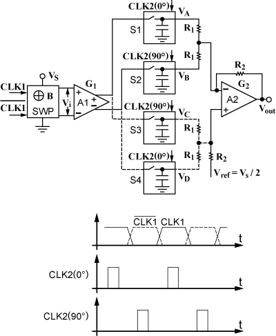
图 5。霍尔装置框图。
差分-差分放大器 A1 将信号 Vi 放大 G1 倍,此信号包括准直流偏移电压加上开关霍尔板所产生的交变有用霍尔信号。在传统斩波放大器中,通过放大器(放大器再次反转复合信号的极性)后的其他开关以及进一步低通滤波来恢复有用信号并消除偏移。
在此应用中,在低磁通密度水平下,Vop ⁄ VH 比率可能达到较高的值,因此要减小残余交流纹波,需要一个成本高昂的多极低通滤波器。例如,为确保在最糟糕的情况下(Vop= 10 mV 且 VH= 0.25 mV)峰-峰纹波最多为 20%,方形偏移电压的基波分量必须衰减 52 dB。在 150 kHz 时钟频率和 34 kHz 带宽下运行时,必须使用四极低通滤波器。此外,有用信号可能被直流分量损害,在每个板开关时,大脉冲产生的直流分量可能会经过低通滤波器。
在 A1 的输出使用两个 S/H 电路 S1 和 S2(分别由 CLK2(0°) 和CLK2 (90°) 提供时钟)可以规避这一问题。这种情况会在 0° 和 90 °状态时发生:一旦板换向瞬变结束所需的延迟时间已经过去 [11]。
假设采样/保持 (S/H) 功能很理想,且 S/H 输出位置的偏置电压是直流信号,则无需进一步过滤会带来高偏移的交流纹波,放宽了输出低通过滤要求。此外,信号不存在寄生脉冲时,采样器的信号同步采样可提高信号恢复过程的精度,尤其是在低电平时。
输出噪声主要是霍尔板电阻的热噪声所致。与传统斩波器相比,由于进入基带的高频噪声分量的“折回”较高,当前方法中的 S/H 功能产生的噪声功率谱密度更高。
回顾方程 3a 和 3b,假设 S/H 功能很理想,注意 S/H 输入是 A1 的互补输出,则 S/H 输出 VA 和 VB(忽略共模 (CM) 信号)为下式提供的直流电压:
VB = ½G1 [VH − |Vop (90°)| − |VoA | ]。 (7)
将 2 输入求和运算放大器 A2(增益 G2= −R2 ⁄ R1)的信号反转,以添加这两个直流电压,然后插入静态输出电压 VQo,忽略 A2 偏移,得到输出:
= VQoi + ½G1 × G2 × Vop(r) + G1 × G2 × VH (8a)
或者
其中,VQoi= Vref= Vs ⁄ 2 是 Vop(r)= 0 时理想的静态输出电压,VQo 是实际静态输出电压。请注意,不良残余偏移的放大值 ½G1×G2是有用信号值的一半。
除 Vop (r) 之外,还有其他分量没有消除,这会使 VQo 偏离其理想值,例如因反馈放大器、电阻网络和 S/H 不匹配发生的偏移。由于在一定温度下可通过晶片修正技术令总偏移量为零,受温度及生产偏差(特别是封装产生的应力)影响的偏移仍然是传感器 IC 面临的最关键问题。
为了减少 S/H 缺陷(如电荷馈通、下垂、非线性)的影响,最终单片传感器 IC 使用全差分 S/H 配置,此配置包括四个 S/H 电路 S1 到 S4 以及一个求和反馈差分输出放大器,如图 5 中的虚线所示。采用这种方式,沿着整个系统对信号进行差分处理。
- 运算放大器 A1 是一个开路放大器,其双极差分装置使用差分电阻负载,如图 6 所示。通过负反馈回路来稳定静态输出电压,负反馈回路由 Q5、 Q6、 M5、 M6、 M7 组成。与闭环放大器相比,开环方法不需要稳定电容器,从而避免了因转换速率限制而引发的稳定时间退化。
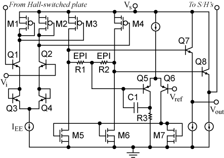
图 6。第一个放大器 A1。
注意,应避免不良饱和效应增加放大器稳定时间,以至于超出之前讨论的霍尔板的稳定时间,并因而降低允许的最大开关频率。为此,将一个增益抑制回路集成到放大器中,此回路包含一个简单的门控 CMOS 通晶体管,可在霍尔板开关转换期间对 Q7 和 Q8 的基极短路。
虽然与 Vop(r) 相比,最大增益是一个可减小后置放大器偏移效应的可取特点,但为了增加线性输入范围,对输入级进行了发射极退化。对于最大输入摆动,线性度高于 99.9%。
使用二极管来实现发射极退化,以令级跨导正比于 IEE ⁄ Vt,从而实现 IEE 的简单线性调整。通过使用 PTAT(与绝对温度呈比例关系)发射极电流偏置,级跨导与温度无关,而 Epi 负载电阻(类似于 Epi 板)使放大器增益随温度变化,因为(迁移率)–1 消除了霍尔元件的迁移率并降低了温度对传感器 IC 灵敏度的影响。
在任何斩波放大器中,斩波频率越高,则滤波电容越小。因此,为减小芯片面积,选择的斩波频率为 170 kHz,这个频率与霍尔板过渡时间允许的最大频率很接近。
放大器典型增益为 30 ×,–3 dB 频率为 4 MHz,0.01% 稳定时间为 400 ns。因此,偏移方波信号被放大,而频率失真可以忽略不计。
- 在信号电平执行 S/H 功能,此电平是输入电平的 G1 倍,这使得 S/H 缺陷的不良影响变得不太明显,之前提到的差分 S/H 排列进一步消除了这些缺陷。
为降低成本,采用开环电路实现 S/H 元件,由高 β 横向 PNP (LPNP) 双极晶体管 Q3 来对接地保持电容器进行传感,如图 7 所示。晶体管 Q1、Q2 和 Q4 有助于减少 Q3 基极电流,从而减少下垂效应。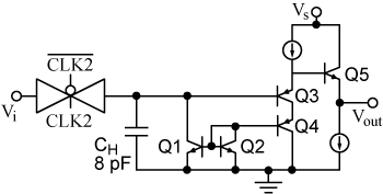
图 7。S/H 电路结构。
- 输出轨至轨反馈放大器是一个相当传统的运算放大器。它的典型增益为 6×,可以为负载提供最大 2 mA 的电流。20 pF 的内部反馈电容可稳定环路并将带宽限制为≈30 kHz。这种后采样窄带技术降低了在高工作频率时典型的输出阶梯纹波和输出白噪声。
IV.单片实现
采用 2–µm BiCMOS 工艺,在单片 IC 上实现 ±0.1 T 全量程线性霍尔器件(使用动态偏移消除技术)和之前描述的基本电路。电源电压为 5 V ±10%,不使用内部稳压器,因为在线性传感器 IC 的很多应用中,尤其是在汽车环境中,灵敏度最好与电源电压成比例关系。此比率功能允许将传感器 IC 输出直接串联到来自同一个电源的模数转换器。此霍尔器件不使用外部组件,而是封在 3–引脚塑料封装中,并且在 –40°C 至 150°C 温度范围运行。
为降低磁灵敏度的生产偏差,利用一个 4 位二进制加权熔断连接网络来调节 IEE,以调整 G1 增益(图 6)。同样,通过另一个熔断网络来调整总电路残余偏移,因为此偏移会影响静态输出电压。这两项调整都是在同一个基准温度的晶片级别上执行的。
图 8 展示的芯片的尺寸为 1.5 × 1.5 mm。霍尔 Epi 板的尺寸为 160 × 160 µm,位于芯片的几何中心。三个时钟信号CLK1、CLK2(0°),和 CLK2(90°) 均来自一个主振荡器,并且都在片上生成。
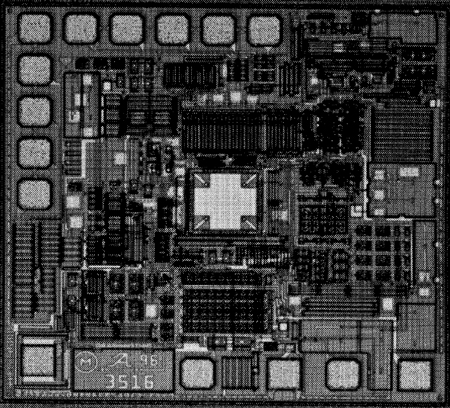
图 8。霍尔传感器 IC 晶片的显微图。晶片尺寸为 1.5 ×1.5 mm。
低电平模拟和 5-V 数字信号使用同一个芯片,并精心布局,以尽可能减小进入敏感区域的数字馈进,从而最大限度地消除残余输出数字噪声。
V. 实验结果
表 I 提供了 TA = 25°C 时最终封装霍尔器件的典型特性。
表 I
| Vsupply | 5 V |
| Isupply | 7 mA |
| Iout(max) | 2 mA |
| 灵敏度 | 25 V ⁄ T |
| 满刻度 | ±100 mT |
| 静态输出电压 | 2.5 V |
| 等效磁偏移量 | 0.5 mT |
| 线性度 | 99.9% |
| 输出噪声 * | 1 mVrms |
| 带宽 | 30 kHz |
*Vsupply 导线利用 0.1 µF 电容器来退耦。
图 9 展示了所测量的霍尔器件的传递函数V= ƒ(B)。通过获取理想直线的最佳拟合的近似值来测量的线性度高达 99.9%。
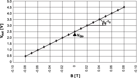
图 10 和 11 展示了在 –40° 到 150°C 完整环境温度范围内作为温度的函数的 VQo 的性能以及总灵敏度S。
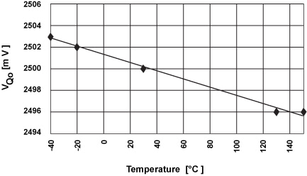
图 10。随温度变化的典型静态输出电压。
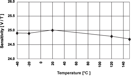
图 11。随温度变化的典型灵敏度。
总输出残余偏移可通过在晶片级别测量 VQo 与 Vref 之间的差值推导出来(参见图 5)。25°C 时的测量结果显示偏移值在 5 到 20 mV 之间,即 0.2 到 0.8 mT。在25°C 时,VQo 的 2.5-V 晶片调整值在封装后几乎没有变化。图 10 所示的 VQo 在其他温度时与 25°C 时的偏差代表了偏移电压中的温度引发漂移。全温度范围的典型的总漂移为 ≈7 mV,这相当于≈0.3 mT 的磁场强度。初步生产数据显示在仅为 ±10 mV 的静态输出电压中的偏差仅为 3σ。在使用多板静态偏移消除技术时,这些偏差(主要由封装引发的应力所致)可能会大得多,因而会降低传感器 IC 的零点基准稳定性。
图 12 展示了灵敏度随着供电电压的变化而变化。
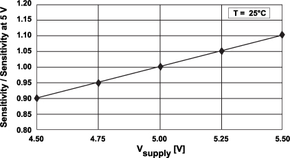
图 12。随供电电压变化而变化的典型灵敏度。
图 13 展示 B = 0 时的霍尔器件输出,拍摄的示波器照片采用的时基与时钟频率同步。它表明,由于片上 S/H 滤波操作,CLK 频率残留可以忽略不计,在输出中留下的高频成分只是霍尔板电阻生成的随机噪声所致。因此,无需外部低通滤波器。如果需要,可在输出增加外部低通滤波来进一步减少输出噪声,这样还可以减小系统带宽。
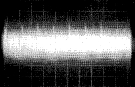
图 13。系统输出噪声,在Vsupply 导线采用 0.1 µF 去耦电容时测得。垂直灵敏度 2 mV ⁄ div。水平灵敏度 1 µs ⁄ div。时基与 CLK 频率同步。
最后,图 14 展示了正弦磁通密度对应的传感器 IC 输出电压。
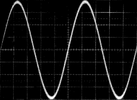
图 14。400 Hz 正弦磁通密度的输出波形。垂直灵敏度 50 mV ⁄ div。水平灵敏度 0.5 ms ⁄ div。磁通密度幅值:8 mT.
VI.结论
本文介绍的 ±0.1 T 单片霍尔线性传感器 IC 使用动态切换功能,配有两对触点和两个切换状态,对于减小传感器 IC 的温度偏移漂移和偏差重现性,这似乎是一个很有吸引力并且具备成本效益的选项。由于在某个基准温度很容易在晶片级别去除偏移,因此在塑料封装的器件中,温度偏移漂移及其重现性成为影响传感器 IC 零点稳定性的最关键问题。在这方面,目前的器件在塑料封装后所展现的零电平稳定性可以与通常使用的多板直流方法相媲美。
相对较小的芯片尺寸证明这种技术的性价比很高,特别是用 S/H 电路(代替常规斩波器的大体积低通滤波器)执行有用信号的恢复和偏移消除时,这种优势更明显。S/H 电路也有助于忽略在板切换期间发生的大换向瞬变,从而可以在非常低的电平下,提供精确和平滑的线性传递函数。
虽然数字和低电平模拟信号使用同一个芯片,但与霍尔板电阻导致的随机噪声相比,输出产生的寄生 CLK 噪声几乎可以忽略不计。
正如文献中所述,较多的板触点对数以及在每个周期切换相位似乎提高了霍尔板的偏移消除能力。当然,此选择方案可能是一项很有意义的挑战,它需要使用在更高频率下运行的更精确的信号调节电路,此电路的偏移应非常小,不会削弱使用复杂板切换获得的优势。
虽然目前的研究对象是线性霍尔传感器 IC,但这些技术同样可用于操作采用“动作”和“释放”开关电平的常用数字传感器 IC。在这种情况下,目前线性传感器 IC 实现的零电平偏差改进可以转换为更好的重现性和切换阈值的温度稳定性。
致谢
作者非常感谢与 J. Higgs、K. Scheller 和 J. Towne 之间的有益讨论,以及 A. Gibbs 进行的广泛实验性工作,他们均在 Allegro MicroSystems 有限公司工作。
参考文献
[1] C. L. Chien and C. R. Westgate, The Hall Effect and Its Applications. New York, NY:Plenum, 1980.
[2] H. P. Baltes and R. S. Popovic, "Integrated semiconductor magnetic field sensors," Proc.IEEE, vol. 74, pp. 1107-1132, Aug. 1986.
[3] G. S. Randhawa, "Monolithic integrated Hall devices in silicon circuits," Microelectron.J., vol. 12, no. 6, pp. 24-29, 1981.
[4] G. Bjorklund, "Improved design of Hall plates for integrated circuits," IEEE Trans.Electron Devices, vol. ED-25, pp. 541-544, May 1978.
[5] Y. Kanda and M. Migitaka, "Effect of mechanical stress on the offset voltage of Hall devices in Si IC, " Phys.Status Solidi (a), vol. 35, pp. K115-K118, 1976.
[6] ----------, "Design considerations for Hall devices in Si IC," Phys.Status Solidi (a), vol. 38, pp. K41-K44, 1976.
[7] J. T. Maupin and M. L. Geske, "The Hall effect in silicon circuits," in The Hall Effect and its Applications, C. L. Chien and C. R. Westgate, Eds.New York, NY:Plenum, 1980.
[8] P. Daniil and E. Cohen, "Low field Hall effect magnetometry," J. Appl.Phys., vol. 53, no. 11, pp. 8257-8259, Nov. 1982.
[9] P. J. Munter, "A low offset spinning-current Hall plate," Sensors and Actuators, vols. A21-A23, pp. 743-746, 1990.
[10] R. Gottfried-Gottfried, "Ein CMOS Hall Sensor mit 8 Kontakten zur Anwendung des Principes der Stromrichtungsumkehr," Sensor 93 Kongressband V, pp. 203-210.
[11] 美国专利号 08 569 814。

1948 年,Alberto Bilotti (S'45–A'48–SM'65–LS'91) 在阿根廷的拉普拉塔大学获得电子工程学学位。
他曾在飞利浦(阿根廷)公司工作七年,在 IBM(法国)公司工作五年,在斯普拉格电气(美国)公司工作三年。他的主要工作是彩色电视机设计、记忆体和 PBX 的高级开发以及模拟 IC 的设计。从 1975 年到 1985 年,他负责阿根廷 Fate 计算机公司的研发工作&。目前,他是模拟-数字 IC、智能功率 IC 以及磁传感器领域的顾问。

1968 年,Gerardo Monreal 出生于阿根廷的布宜诺斯艾利斯。1994 年,他从阿根廷的布宜诺斯艾利斯大学获得电子工程学学位。
他开始在布宜诺斯艾利斯从事神经网络工作。1992 年,他加入了 Electrónica Bilotti 并担任 IC 设计工程师。目前,他的工作重点是模拟-数字 IC 和磁智能传感器 IC。

Ravi Vig 出生于印度孟买。1982 年,他获得新泽西州新不伦瑞克省的罗格斯大学获得学士(电子工程)学位,并于 1984 年,获得新罕布什尔州达特茅斯学院于获得硕士学位(电子工程)。
从 1984 年 10 月起,他先在 Sprague Electric 工作,之后在马萨诸塞州伍斯特市的 MicroSystems 公司,担任霍尔效应集成电路产品 IC 设计师和 IC 设计经理。他的工作领域包括耐高温霍尔传感器 IC、多路复用传感器 IC 以及自动校准齿轮传感器 IC。他还曾担任 Automotive Products 的战略营销经理。他目前担任 Allegro MicroSystems 有限责任公司业务开发部的副总裁
1996 年 7 月 26 日收到稿件;1996 年 11 月 28 日校订。本文获得马萨诸塞州伍斯特市的 Allegro MicroSystems 有限公司的支持。
A. Bilotti 和 G. Monreal 均在阿根廷的 Electrónica Bilotti, Olivos 1636 工作。
R. Vig 在美国马萨诸塞州伍斯特市的 Allegro MicroSystems, 有限公司工作。
出版商项目标识符 S 0018 9200 (97) 03841-9。0018-9200/97$10.00 © 1997, IEEE
本文描述的产品 A3515xUA 和 A3516xUA 是用于高温环境的比率线性霍尔传感器 IC。
本文最初发表于 IEEE 杂志《固态电路》第 32 卷第 6 期,1997 年 6 月。转载需经许可。
STP97-10
使用动态正交偏移消除的单片磁性霍尔传感器 IC
By Alberto Bilotti, Life Senior Member, IEEE, Gerardo Monreal, and Ravi Vig
Abstract—The offset voltage, and its temperature drift and production spread, which generally degrades the zero-level stability and reproducibility of magnetic Hall sensor ICs, can be reduced using a single Hall plate and switching means for periodic permutation of the supply and output contact pairs. The present work describes a chopper-based 5-V monolithic linear Hall sensor IC with a ±0.1 T full scale where this dynamic plate offset cancellation technique has been employed together with a cost-effective signal conditioner. The device was integrated using a 2-µm conventional BiCMOS process and the final chip, measuring 1.5 × 1.5 mm, shows, after packaging in a 3-pin plastic package, a residual offset with a production spread and a temperature-induced drift five to ten times smaller than in currently used multiplate DC quadrature cancellation approaches. The device does not require external components and provides an output free of HF residues.
Index Terms—BiCMOS analog integrated circuits, choppers, Hall devices/effect, microsensors, monolithic integrated circuits.
I. INTRODUCTION
MONOLITHIC magnetic sensor ICs generally use Si Hall elements which are integrated simply with the amplifier or signal-conditioner circuits required for amplification or processing the relatively low voltages generated. The Hall effect, its characteristics, applications, etc., have been extensively dealt with in the literature [1]−[3]. An excellent review with many references can be found in Baltes' and Popovic's work.
The simplest Hall element uses a square plate made, for example, of an Epi-pocket in a bipolar or BiCMOS process with two pairs of orthogonally-oriented contacts, as shown in Fig.1. When a supply voltage Vs is applied across one pair of contacts, for example a, c, a magnetic flux density B normal to the plate generates a voltage VH across the other pair b, d, such that
where Sv is the Hall element sensitivity per unit supply voltage. The sensitivity given by VH ⁄B × Vs [T-1], where T (tesla; 1 T = 1 × 10⁴gauss) is the meter-kilogram-second (mks) unit for magnetic flux density (induction), is approximately a constant parameter, depending only on the Si layer mobility and the plate and contact geometries. Typical values of Sv range between 0.04 and 0.08 T-1, which means, for a typical 5-V supply and minimum magnetic flux density of 1 mT, output voltages of 200 to 400 µV.
Fig. 1. Basic Hall plate.
In all DC applications, the minimum magnetic flux density capable of being accurately measured by such plates depends on the offset voltage Vop appearing at the plate output contacts for B = 0. The plate, from an electrical point of view, will show unavoidable imbalances due to resistance gradients, geometrical asymmetries [4], piezoresistive effects [5], [6], etc., generating a nonnegligible offset voltage. As the plate offset Vop is relatively large—it may range from 0.5 to 5 mV for a 5-V supply and is temperature-, supply voltage-, and stress-dependent—efforts have been made for cancelling or minimizing its effects.
Offset cancellation cannot be performed by such switching techniques as those used in amplifiers, as there is no available state where Vop could be isolated from VH except cutting off the magnetic field, which is certainly a nonviable proposal.
Noting that, from a DC point of view, the Hall plate can be viewed as a distributed resistive Wheatstone bridge, most present commercial Hall sensor ICs cancel the offset by using two or more appropriately interconnected plates where the electrical current direction is 90° rotated from one plate to the other [7]. If the imbalance source remains invariant and fixed in the solid space, the offsets of any pair of plates will be equal but of opposite polarity, achieving the desired cancellation. On the other hand, the useful signal of the multiplate arrangement remains equal to that of a single plate.
Alternatively, the use of only one plate while generating the quadrature states by periodic supply and output contact permutations has been proposed [8], [9]. Although this dynamic offset cancellation technique requires a more complicated signal conditioner following the Hall switched-plate, it has the advantage of reducing the residual offset and its production spread as compared with multiplate sensor ICs. In the last case, the zero-level deviations are degraded due to plate offset mismatches between physically different plates, these mismatches being mostly generated by the plastic package temperature-dependent built-in stresses.
This work describes 5-V BiCMOS monolithic linear Hall sensor ICs using the dynamic offset cancellation technique, where the various functions required for recovering the useful signal and cancelling the offset are performed by a cost-effective signal conditioner.
A BiCMOS technology was preferred in order to have simple high-gain open-loop amplifiers with low offset, accurate temperature-programming circuits, as well as a low-cost high-output current sourcing capability.
II. THE SWITCHED HALL PLATE
The simplest dynamic offset cancellation technique uses a single square plate with four contacts where the quadrature states are generated by periodically connecting the supply voltage and supply conditioner input to one pair of contacts or to the other, as shown in Fig. 2. Each state, which we shall call from now on the 0° state or the 90° state, is defined by the complementary clocks CLK1 and CLK1_bar, respectively.
Fig. 2. (a) In a dynamic offset cancellation technique, the current flowing through the plate is periodically switched from the 0° to the 90° direction and vice versa. (b) Clock, Hall voltage, and plate offset waveforms.
Assuming B = 0 and an ideal Wheatstone bridge model for the Hall plate, the voltages appearing at the output contacts are the plate offsets Vop(0°) and Vop(90°) which are equal in magnitude but have opposite polarities. This can be verified in a very simple way as follows. Assume that an imbalance, for example due to a stress pattern, occurs such that the region between contacts a and b shows a resistivity smaller than the rest of the plate (dotted resistor in Fig. 2), and that this situation does not change when changing states. Then, the offsets developed at each state have the same magnitude but opposite polarities, as the same imbalance occurs in adjacent branches of the equivalent bridge network (the Hi terminal will be more positive than the Lo terminal in the 0° state but more negative in the 90° state).
For B ≠ 0, as the supply and output connections rotate in the same direction, VH keeps its polarity unchanged, making VH invariant. This characteristic of VH derives from the antireciprocal property of a symmetrical Hall plate.
There appears, therefore, a simple way to discriminate the offset from the useful signal and further cancelling the offset by appropriate signal conditioning. Although in Fig. 2, VH is quasi-constant and Vop an alternating square wave, waveforms can be interchanged if desired by interchanging output contacts a and c during the 90° state.
As an ideally perfect cancellation is never possible, there is in practice a residual plate offset Vop (r) defined as
where absolute values have been preferred for emphasizing the polarity reversals occurring during further signal processing. Depending on the fabrication process, the Hall plate geometry and crystallographic orientation, and the residual wafer and package stresses, Vop(r) may range between 50 and 500 µV for a 5-V supply.
DC measurement data of a quadrature cancellation on a single plate, either in an Epi plate [9] or in an MOS channel "plate" [10], showed an appreciable improvement as compared to the conventional multiplate approach. For reducing Vop(r) these measurements were performed in plates using four pairs of contacts distributed around the periphery of a circular plate as in a "spinning" Hall cell [9]. In this case, multiplexed addition of all possible offsets for improving cancellation would require eight switching states per cycle.
For simplifying purposes and reducing chip area, the simplest approach of the Epi plate with two pairs of contacts and two phases per cycle as shown in Fig. 2 was chosen for our monolithic sensor IC.
The maximum allowable plate switching frequency depends on the plate voltage settling time after each commutation transition. Note that, for example, after the transition from the 0° state to the 90° state, the voltage Va at contact a in Fig. 2 has to decay from Vs to Vs ⁄ 2, and Vc has to increase from zero to Vs ⁄ 2 (while voltages at d and b have to decay to ground and increase to Vs, respectively). This requires a rearrangement of charges stored in the Epi-Sub reversed-biased junction and therefore, a certain time for voltages to settle down into the final value Vs ⁄ 2, after which the Hall output voltage will be valid and ready to be processed, as shown in Fig. 3.
Fig. 3. 0° state to 90° state Hall plate switching transient where Va and Vc are the voltages at contacts a and c in Fig.2.
Switching measurements, of a Hall plate built on a square Epi layer that was 2 Ω-cm, 5.5 µm thick, with 3 kΩ resistance between diagonal-opposite facing contacts, showed that the Hall voltage will be valid only after ≈600 ns have elapsed from the plate commutation transition. Taking into account component tolerances and the fact that additional sample pulses must be included in each phase, a maximum plate switching frequency of 200 kHz was found. As long as the switching frequency remains below this limit, the switching frequency is not critical for the system operation, simplifying, therefore, the implementation of the clock circuitry.
Even if there would be a residual voltage due to an excessive settling time, this voltage would remain invariant during both states, just as the true offset does, and therefore would be cancelled out. This has not been exploited further as it requires a very accurate and more costly CLK generator.
Fig. 4 shows the actual switched-plate arrangement used in the monolithic sensor IC where the four single-pole double-throw (SPDT) switches required for the contact permutation were implemented with MOS transistors. The plate contact interconnections follow the basic scheme of Fig. 2 except for an interchange of the output terminals during the 90° state. With this arrangement, at each change of state, VH changes polarity and Vop remains quasi-constant, in such a way that VoA, the DC input-referred offset of amplifier A1, will become indistinguishable from Vop, and the Hall plate and the input amplifier offsets will be simultaneously processed and cancelled by the signal conditioner.
Fig. 4. Switched Hall plate. When the CLK1 signal is high, current flows between a and c (0° state) and when CLK_bar is high, current flows between b and d (90° state).
Thus, the A1 offset is cancelled at no cost, avoiding the extra hardware required to perform the same function by other techniques such as autozero, signal conditioning (SC), etc.
The input voltages to the ideal amplifier A1 become
Vi (90°) = −VH + |Vop (90°)| + |VoA | during 90° state. (3b)
For avoiding degrading Vop(r) through eventual mismatchings between the supply voltages effectively applied to the plate during each phase, transistors M1 through M4 were properly sized so as to keep their on-voltage drop below 100 mV.
Taking into account that the total offset Vop + VoA must be amplified without distortion by A1, dynamic range considerations require minimizing VoA, therefore suggesting the use of a low-offset differential bipolar input stage. In this case, base input currents Ib flowing through MOS switches M5 through M8 may generate a residual offset VoI (r) additional to that given by equation 2. Assuming ΔIb «Ib, straightforward calculation gives
where
As A1 uses a conventional base current cancellation circuitry, VoI (r) is smaller than 2 µV and, therefore, can be fully neglected as compared to Vop(r).
III. SIGNAL CONDITIONER
Fig. 5 is a simplified block diagram of the complete linear Hall device, where the previously described switched-Hall plate is represented by block SWP. Note that for zero offset and B = 0, the output amplifier A2 has its quiescent output voltage, VQoi, defining the sensor zero level, at Vs ⁄ 2. The signal conditioner operates as a quasi-chopped amplifier where the first pair of cross-coupled switches are built in the switched Hall plate, and where the second pair of switches plus the conventional low-pass (LP) filter have been substituted by sample and hold (S/H) and adding functions, as described next.
Fig. 5. Hall device block diagram.
The differential-differential amplifier A1 amplifies G1 times the signal Vi comprising the quasi-DC offset voltage plus the alternating useful Hall signal generated by the switched Hall plate. In conventional chopper amplifiers, the useful signal is recovered and the offset cancelled by additional switches after the amplifier, that inverts again the composite signal polarity, and by further LP filtering.
In this application, as at low magnetic flux density levels, the Vop ⁄ VH ratio may attain high values, a costly multiple-pole LP filter is required for reducing the residual AC ripple. For example, for insuring a maximum peak-to-peak ripple of 20% in the worst case of Vop = 10 mV and VH = 0.25 mV, the fundamental component of the square-shaped offset voltage must be attenuated 52 dB. When operating at a clock frequency of 150 kHz with a bandwidth of 34 kHz, a four-pole LP filter is required. Besides, the useful signal may be corrupted by DC components, generated by the large pulses occurring at each plate switching, that may go through the LP filter.
The problem was circumvented by using, at the outputs of A1, two S/H circuits S1 and S2, which are clocked by narrow pulses CLK2(0°) and CLK2(90°), respectively. This occurred during the 0° and 90° states, once the required delay for the plate commutation transients to die out had elapsed [11].
Assuming an ideal S/H function, the offset voltages at the S/H outputs are DC signals, and there is no need any more to further filter out the otherwise high offset AC ripple, relaxing the output LP filtering requirements. Also, the synchronous sampling of the signal by the samplers when the signal is free of spurious pulses improves the accuracy of the signal recovery process, particularly at low levels.
As far as the output noise is concerned, this is mainly due to the thermal noise of the Hall plate resistance. When compared to a conventional chopper, the S/H function in the present approach produces a higher noise power spectral density at low frequencies due to a higher "fold-back" of HF noise components into the baseband.
Recalling equations 3a and 3b, assuming ideal S/H functions and noting that the S/H inputs are complementary outputs of A1, the S/H outputs VA and VB are, neglecting common mode (CM) signals, DC voltages given by
VB = ½G1 [VH − |Vop (90°)| − |VoA | ]. (7)
Adding these two DC voltages, by means of the inverting two-input summing op-amp A2, with gain G2 = − R2 ⁄ R1, and then inserting the quiescent output voltage VQo, produces, neglecting A2 offset contributions, the output
= VQoi + ½G1 × G2 × Vop(r) + G1 × G2 × VH (8a)
or
where VQoi = Vref = Vs ⁄ 2 is the ideal quiescent output voltage for Vop(r) = 0 and VQo the actual quiescent output voltage. Note that the amplification ½G1 × G2 of the undesirable residual offset is half that of the useful signal.
Apart from Vop(r), there are other components that remain uncancelled and that will shift VQo from its ideal value, such as offsets due to the feedback amplifier, resistor networks, and S/H mismatchings, etc. As the total offset can be nulled at one temperature by any wafer-trimming technique, the offset drift with temperature and its production spread, particularly due to package-induced stresses, remain the most critical sensor IC issues.
For reducing the effects of S/H imperfections such as charge feedthrough, droop, nonlinearity, etc., the final monolithic sensor IC uses a fully differential S/H configuration comprising four S/H circuits S1 to S4 and a summing feedback difference output amplifier, as shown with dotted lines in Fig.5. In this way, the signal is differentially processed all along the whole system.
- Amplifier A1 is an open-loop amplifier with a bipolar input differential stage using differential resistive loads, as shown in Fig. 6. The quiescent output voltage is stabilized by means of a negative feedback loop comprising Q5, Q6, M5, M6, and M7. As compared to a closed-loop amplifier, the open-loop approach does not require stability capacitors, avoiding any settling time degradation due to slew rate limitations.
Fig. 6. First amplifier A1.
Care was exercised to avoid undesirable saturation effects increasing the amplifier settling time beyond the plate settling time previously discussed, decreasing the maximum allowable switching frequency. For this, a gain-killer circuit comprising a simple gated CMOS pass transistor that short-circuits the bases of Q7 and Q8 during the Hall plate switching transitions was incorporated into the amplifier.
Although maximum gain is a desirable feature for reducing the effect of post-amplifier offsets as compared to Vop(r), the input stage was emitter-degenerated for increasing the linear input range. The linearity, for the maximum input swing, is better than 99.9%.
Diodes were used for emitter degeneration for keeping the stage transconductance proportional to IEE ⁄ Vt, allowing simple linear adjustment of IEE. By using a PTAT (proportional to absolute temperature) emitter current bias, the stage transconductance becomes temperature independent, while the Epi load resistors, similar to the Epi plate, make the amplifier gain vary with temperature as (mobility)–1 cancelling the Hall sensitivity mobility dependance and reducing the sensor IC sensitivity variations with temperature.
In any chopping amplifier the higher the chopping frequency the smaller the filter capacitors. Consequently, for reducing the chip area, a chopping frequency of 170 kHz, close to the maximum allowed by the Hall plate transition times, was chosen.
The amplifier has a typical gain of 30×, a –3 dB frequency of 4 MHz, and a 0.01% settling time of 400 ns. The offset square wave signal is therefore amplified with negligible frequency distortion.
- The S/H function is performed at signal levels G1 times higher than the input level, making the undesirable effects of S/H imperfections less noticeable, these imperfections being further cancelled by the differential S/H arrangement previously mentioned.
For cost-reduction purposes, the S/H elements were implemented as open-loop circuits, the grounded holding capacitor being sensed by a high-beta lateral-PNP (LPNP) bipolar transistor, Q3 as shown in Fig. 7. Transistors Q1, Q2, and Q4 help reducing Q3 base current, reducing therefore the droop. Fig. 7. S/H circuit configuration.
- The output rail-to-rail feedback amplifier is a rather conventional op-amp. It has a typical gain of 6× and is capable of sourcing a maximum of 2 mA into the load. An internal feedback capacitor of 20 pF stabilizes the loop and limits the bandwidth to ≈30 kHz. This post-sampling narrowbanding reduces the typical output staircase ripple at high operating frequencies and the output white noise.
IV. MONOLITHIC IMPLEMENTATION
A ±0.1 T full scale linear Hall device using dynamic offset cancellation and the basic circuits previously described was implemented in a monolithic IC using a 2–µm BiCMOS process. The supply voltage is 5 V ±10%, and no internal voltage regulator is used because in many applications of linear sensor ICs, particularly in the automotive environment, the sensitivity should preferably be proportional to the supply voltage. This ratiometric feature allows cascading the sensor IC output directly to an A-to-D converter fed from the same supply. The device uses no external components, is packaged in a 3–pin plastic package, and operates within a –40°C to 150°C temperature range.
In order to reduce the production spread of the magnetic sensitivity, gain G1 is trimmed by adjusting IEE (Fig. 6) with a 4-bit binary-weighted fuse-link network. Similarly, the total circuit residual offset, affecting the quiescent output voltage, is trimmed out by another fuse-link network. Both adjustments are performed at the wafer level at one single reference temperature.
The chip, measuring 1.5 × 1.5 mm, is shown in Fig. 8. The Hall Epi plate, measuring 160 × 160 µm, is located at the chip geometric center. The three clock signals CLK1, CLK2(0°), and CLK2(90°) are derived from a master oscillator, and are generated on-chip.
Fig. 8. Microphotograph of the Hall sensor IC die. Die size is 1.5 × 1.5 mm.
As low-level analog and 5-V digital signals share the same chip, layout precautions were taken for minimizing digital feedthrough into sensitive areas, therefore minimizing any residual output digital noise.
V. EXPERIMENTAL RESULTS
Table I gives the measured typical characteristics of the final packaged Hall device at TA = 25°C.
TABLE I
| Vsupply | 5 V |
| Isupply | 7 mA |
| Iout(max) | 2 mA |
| Sensitivity | 25 V ⁄ T |
| Full scale | ±100 mT |
| Quiescent output voltage | 2.5 V |
| Equivalent magnetic offset | 0.5 mT |
| Linearity | 99.9% |
| Output noise* | 1 mVrms |
| Bandwidth | 30 kHz |
*Vsupply lead decoupled with a 0.1 µF capacitor.
Fig. 9 shows the measured Hall device transfer function Vout = ƒ(B). The linearity, measured as an approximation to the best fit to an ideal straight line, amounts to 99.9%.
Fig. 9. Measured transfer function Vout = ƒ(B) at 25°C.
Figs. 10 and 11 show the performance of VQo, and total sensitivity S, as functions of temperature within the full ambient temperature range –40°C to 150°C.
Fig. 10. Typical quiescent output voltage variation with temperature.
Fig. 11. Typical sensitivity variation with temperature.
The total output residual offset can be derived by measuring the difference between VQo and Vref (see Fig. 5) at the wafer level. Measurements at 25°C show offsets ranging from 5 to 20 mV, i.e., from 0.2 to 0.8 mT. The 2.5-V wafer-trimmed value of VQo at 25°C remains practically unchanged after packaging. The VQo deviation at other temperatures from its reference value at 25°C, shown in Fig. 10, represents a temperature-induced drift in the offset voltage. The typical total drift for the full temperature range is ≈7 mV, equivalent to a magnetic field of ≈0.3 mT. Preliminary production data show a 3σ spread in the quiescent output voltage of only ±10 mV. When using multiplate static offset cancellation techniques, these deviations, mainly caused by package-induced stresses, can be much larger, degrading the sensor IC zero reference stability.
Fig. 12 shows the sensitivity variation with the supply voltage.
Fig. 12. Typical sensitivity variation with supply voltage.
Fig. 13 gives the Hall device output for B = 0, the oscilloscope photo being taken with the timebase synchronized to the clock frequency. It shows that due to the on-chip S/H filtering action, the CLK frequency residue is negligible and the main HF components left at the output are only those due to the random noise generated by the Hall plate resistance. Consequently, no external LP filter is required. If desired, the output noise can be further reduced by additional external LP filtering at the output, reducing at the same time the system bandwidth.
Fig. 13. System output noise, measured with a 0.1 µF decoupling capacitor at the Vsupply lead. Vertical sensitivity 2 mV ⁄ div. Horizontal sensitivity 1 µs ⁄ div. Timebase synchronized to CLK frequency.
Finally, Fig. 14 shows the sensor IC output voltage for a sinusoidal magnetic flux density.
Fig. 14. Output waveform for a 400 Hz sinusoidal magnetic flux density. Vertical sensitivity 50 mV ⁄ div. Horizontal sensitivity 0.5 ms ⁄ div. Magnetic flux density amplitude: 8 mT.
VI. CONCLUSIONS
The described ±0.1 T monolithic Hall linear sensor IC using dynamic switching with two pairs of contacts and two switching states appears to be an attractive cost-effective option for reducing the sensor IC offset drift with temperature and the offset reproducibility. As the offset itself is simply trimmed out at the wafer level at one reference temperature, the offset drift with temperature and its reproducibility particularly in plastic-packaged devices becomes the most crucial issue affecting the sensor IC zero stability. In this respect, the present device, after plastic packaging, shows a zero-level stability that compares very favorably with commonly used multiplate DC approaches.
The relatively small chip size proves that this technique can be cost-effective, particularly when recovery of the useful signal and offset cancellation are performed by S/H circuits, substituting for the large-footprint LP filter of a conventional chopper used otherwise. The S/H circuits also help in ignoring the large commutation transients occurring during plate switching, providing an accurate and smooth linear transfer function at very low levels.
Although digital and low-level analog signals share the same chip, the spurious CLK noise developed at the output is almost negligible as compared to the random noise due to the Hall plate resistance.
As suggested in the literature, a higher number of plate contact pairs and switching phases per cycle seems to improve the Hall plate offset cancellation. Certainly this option could be an interesting challenge, requiring a more refined signal-conditioning circuitry operating at higher frequencies and showing an offset sufficiently small not to compromise the advantages gained by the more sophisticated plate switching.
Although the present work deals with linear Hall sensor ICs, the same techniques could be used for implementing the commonly used digital sensor ICs with "operate" and "release" switching levels. In this case, the improvements in the zero level deviations achieved in the present linear sensor ICs will translate into better reproducibility and temperature stability of the switching thresholds.
ACKNOWLEDGMENT
The authors gratefully acknowledge the useful discussions with J. Higgs, K. Scheller, and J. Towne, and the extensive experimental work performed by A. Gibbs, all with Allegro MicroSystems, LLC
REFERENCES
[1] C. L. Chien and C. R. Westgate, The Hall Effect and Its Applications. New York, NY: Plenum, 1980.
[2] H. P. Baltes and R. S. Popovic, "Integrated semiconductor magnetic field sensors," Proc. IEEE, vol. 74, pp. 1107-1132, Aug. 1986.
[3] G. S. Randhawa, "Monolithic integrated Hall devices in silicon circuits," Microelectron. J., vol. 12, no. 6, pp. 24-29, 1981.
[4] G. Bjorklund, "Improved design of Hall plates for integrated circuits," IEEE Trans. Electron Devices, vol. ED-25, pp. 541-544, May 1978.
[5] Y. Kanda and M. Migitaka, "Effect of mechanical stress on the offset voltage of Hall devices in Si IC, " Phys. Status Solidi (a), vol. 35, pp. K115-K118, 1976.
[6] ----------, "Design considerations for Hall devices in Si IC," Phys. Status Solidi (a), vol. 38, pp. K41-K44, 1976.
[7] J. T. Maupin and M. L. Geske, "The Hall effect in silicon circuits," in The Hall Effect and its Applications, C. L. Chien and C. R. Westgate, Eds. New York, NY: Plenum, 1980.
[8] P. Daniil and E. Cohen, "Low field Hall effect magnetometry," J. Appl. Phys., vol. 53, no. 11, pp. 8257-8259, Nov. 1982.
[9] P. J. Munter, "A low offset spinning-current Hall plate," Sensors and Actuators, vols. A21-A23, pp. 743-746, 1990.
[10] R. Gottfried-Gottfried, "Ein CMOS Hall Sensor mit 8 Kontakten zur Anwendung des Principes der Stromrichtungsumkehr," Sensor 93 Kongressband V, pp. 203-210.
[11] U.S. Patent 08 569 814.
Alberto Bilotti (S'45–A'48–SM'65–LS'91) received the degree in electrical engineering from La Plata University, Argentina, in 1948.
He worked with Philips, Argentina for seven years, IBM, France for five years, and Sprague Electric Co., USA, for three years. His main activities were design of color televsions, advanced development in memories and PBXs, and design of analog ICs, respectively. From 1975 to 1985, he was responsible for R&D in Fate Computer Co., Argentina. At present, he is a consultant in the area of analog-digital ICs, smart power ICs, and magnetic sensors.
Gerardo Monreal was born in Buenos Aires, Argentina, in 1968. He received the degree in electronic engineering from Universidad de Buenos Aires, Argentina, in 1994.
He started working on neural networks at the Universidad de Buenos Aires. In 1992, he joined Electrónica Bilotti where he serves as an IC Design Engineer. Currently, his works concern analog-digital ICs and magnetic smart sensor ICs.
Ravi Vig was born in Mumbai, India. He received the B.S. (EE) degree from Rutgers University, New Brunswick, NJ, in 1982 and the M.S. (EE) degree from Dartmouth College, Hannover, NH, in 1984.
He has worked at Sprague Electric and then Allegro MicroSystems Inc., Worcester, MA, since October 1984, as an IC Design Engineer and later as Design Manager for Hall effect integrated circuit products. His activities have included high-temperature Hall sensor ICs, multiplexed sensor ICs, and self-calibrating gear sensor ICs. He has also worked as the Strategic Marketing Manager for Automotive Products. He currently holds the position of Vice President, Business Development at Allegro MicroSystems, LLC
Manuscript received July 26, 1996; revised November 28, 1996. This work was supported by Allegro MicroSystems, LLC, Worcester, MA.
A. Bilotti and G. Monreal are with Electrónica Bilotti, Olivos 1636, Argentina.
R. Vig is with Allegro MicroSystems, LLC, Worcester, MA, USA.
Publisher Item Identifier S 0018-9200(97)03841-9. 0018-9200/97$10.00 © 1997, IEEE
The products described here are the A3515xUA and A3516xUA, ratiometric, linear Hall-effect sensor ICs for high-temperature operation.
This paper was originally published in the IEEE Journal of Solid-State Circuits, Vol. 32, No. 6, June 1997. Reprinted by permission.
STP97-10