Non-Local Model for the Spatial Distribution of Impact Ionization Events in Avalanche Photodiodes
Abstract
An extension of the analytical Dead Space Multiplication Theory [IEEE Trans. Electr. Dev., vol. 39, pp. 546–552, 1992] is reported. This extension provides the means to analytically determine the spatial distribution of electron and hole impact-ionization events in an arbitrarily specified heterojunction multiplication region. The model can be used to understand the role of dead space in regularizing the locations of impact ionization. It can also be used to analyze, design, and optimize new generations of ultra-low-noise avalanche photodiodes with multi-staged gain based on judicious energizing and relaxing of carriers to enhance electron impact ionizations and to suppress hole impact ionizations.
Introduction
Avalanche photodiodes (APDs) are widely deployed in high-data-rate optical-fiber communication and lidar systems that operate at the wavelengths of 1.3 µm. Among the APD structures, the separate absorption, charge and multiplication (SACM) InP-InGaAs APDs have been the preferred structure for two reasons. First, they have high sensitivity, which results from their internal carrier multiplication, namely the avalanche of impact ionizations that result from each photogenerated carrier. Second, they are highly cost effective compared to receivers that employ optical pre-amplification. However, due to the stochastic nature of the impact-ionization process, the multiplication gain comes at the expense of extra noise. This multiplication noise is characterized by a quantity termed “the excess noise factor,” which accounts for the gain uncertainty.
Various approaches have been explored to reduce the excess noise factor of APDs. These approaches include the use of thin multiplication regions and impact-ionization engineered (I2E) multiplication regions. Both approaches exploit the dead-space effect to reduce the excess noise by making the spatial distribution of impact ionizations more deterministic. [1],[2] The dead space is the minimum distance a carrier must travel before it gains sufficient energy from the electric field to cause an impact ionization. Another approach is to suppress the impact ionization of holes (or electrons), β → 0 (or α → 0), to make α and β as dissimilar as possible. According to the local field theory, both the gain-bandwidth product and the excess noise of APDs improve when one of the ionization coefficients is much larger than the other. [3],[4] As such, interest has been growing in APD structures that suppress the impact ionization of holes (or electrons) by impact-ionization engineering of the multiplication region. [5],[6] In these structures, the relaxation of one type of carrier (to prevent it from impact ionizing) is achieved by judiciously engineering the different layers of the heterojunction multiplication region and the electric field profile therein. A key factor in the successful design of multi-layer multiplication regions is the ability to accurately determine the places at which electrons and holes trigger impact-ionization events.
This paper reports an extension of the analytical Dead Space Multiplication Theory (DSMT) [7] that enables determination of the spatial distribution of impact-ionization events within an arbitrarily specified heterojunction multiplication region. The recursive equations reported allow the number of electron and hole impact-ionization events to be determined individually within any subregion of the multiplication region. Moreover, the model can accommodate carrier relaxation, which can be used to suppress the impact ionizations of one type of carrier.
Model
Consider an arbitrary multiplication region that extends from x = 0 to x = w. An impact ionization event that is initiated by a conduction-band electron is called an electron-ionization event; an impact-ionization event that is affected by a valence-band hole is termed a hole-ionization event. The goal is to compute the mean of the total number of electron-ionization events as well as hole-ionization events that occur in a subset after a single parent carrier (at a prescribed location) initiates the avalanche process. If this problem can be solved for any subset A—where A is any subset of the interval [0, w]—then it can be specialized to the intervals A1 = [0, w/n), A2 = [w/n, 2w/n), …, An = [(n – 1)w/n, w], and the distribution of electron- and hole-ionization events throughout the multiplication region can be obtained. (The partition parameter n is selected to achieve a desired spatial distribution resolution.) To solve this problem, Ze(x) and Zh(x) are defined as the total stochastic number of electron impact-ionization events and hole impact-ionization events, respectively, when the avalanche process is triggered by a parent electron at location x. Similarly, Ye(x) and Yh(x) are defined as the total stochastic number of electron impact-ionization events and hole impact-ionization events, respectively, when the avalanche process is triggered by a parent hole at location x.
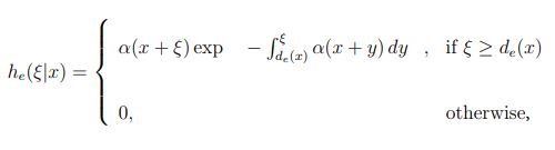
The formulation of recursive equations that enable the ensemble averages of the quantities Ze(x) and Zh(x), Ye(x) and Yh(x) to be solved requires an understanding of the probability density function of the distance from the birth location of a carrier to the location of its first impact ionization thereafter. Following the notation in Hayat, et al., [2], he(ξ|x) denotes the probability density function of the distance, ξ, to the first ionization measured from the electron birth position at x; and similarly, hh(ξ|x) denotes the probability density function of the distance traveled by a hole born at x before it first ionizes. In the DSMT, he(ξ|x) and hh(ξ|x) are described by the shifted-exponential models:
Equation 1:
and
Equation 2:
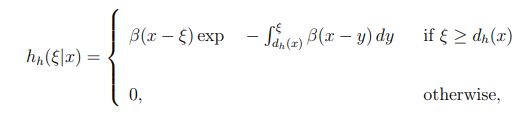
where de(x) and dh(x) are the electron and hole dead spaces, respectively. The exact formulas for calculating the dead space can be found in the work of Hayat, et al. [2]
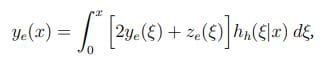
Next, a renewal argument is invoked, similar to that introduced by Hayat, et al., [8] to obtain recursive (integral) equations for the mean of the quantities Ze(x) and Zh(x), Ye(x) and Yh(x), denoted as ze(x) and zh(x), ye(x) and yh(x), respectively. Consider a parent electron at x initiating the avalanche process, and suppose that its first ionization occurs at some location ξ > x.
If it is assumed (for the moment) that ξ∉A, then—given that the first ionization has occurred at ξ—the conditional mean of Ze(x) is simply ze1(ξ) + ze2(ξ) + ye(ξ), where ze1(ξ) and ze2(ξ) are the total average electron ionization events that from the two offspring electrons at ξ, and ye(ξ) is the total average electron ionization events that result from the offspring hole at ξ. On the other hand, if the location ξ of the first ionization is in A, then—at the instance of the first ionization—one electron ionization has already occurred, and this additional electron ionization must be considered. In this case, the conditional mean of Ze(x) is 1 + ze1(ξ) + ze2(ξ) + ye(ξ). In the event that the parent electron does not impact ionize [with probability ∞ ∫w he (ξ|x) d ], then Ze(x) = 0. When all of these scenarios are considered and averaged over all possible locations, ξ, of the location of the first impact ionization (by the parent electron), simplification can be used to obtain the integral equation:
Equation 3:
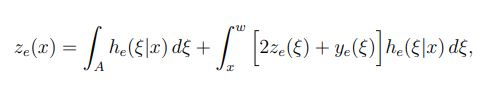
where the first term is simply the probability that the first ionization occurs in region A. The same argument can be repeated to analyze the ensemble averages of the quantities Zh(x), Ye(x), and Yh(x); such analysis leads to three additional integral equations:
Equation 4:
Equation 5:
and
Equation 6:
These coupled recursive equations (Equation 3, Equation 4, Equation 5, and Equation 6) can be solved numerically using a simple iterative method.
Results
The spatial distribution of electron- and hole-ionization events were calculated for two different cases of the multiplication region: 1) a hole-injection InP homojunction multiplication region; and 2) an electron-injection heterojunction multiplication region. Partition parameter n was used, where n = 50 in the case of the homojunction multiplication region, and n = 100 in the case of the heterojunction multiplication region.
The calculated spatial distribution of the impact-ionization events initiated by electrons and holes in an InP homojunction multiplication region of 150 nm under a constant electric field is shown in Figure 1. Parent holes are assumed to be injected at x = 0. The figure shows that the number of hole-impact ionization events increases as the holes approach x = 150 nm, and the number of electron impact-ionizations events increases as the electrons approach x = 0. This result is consistent with the fact that holes and electrons multiply as they acquire sufficient kinetic energy from the electric field as they travel in opposite directions. More importantly, the figure shows the effect of the dead space on the spatial distribution of the impact-ionization events.
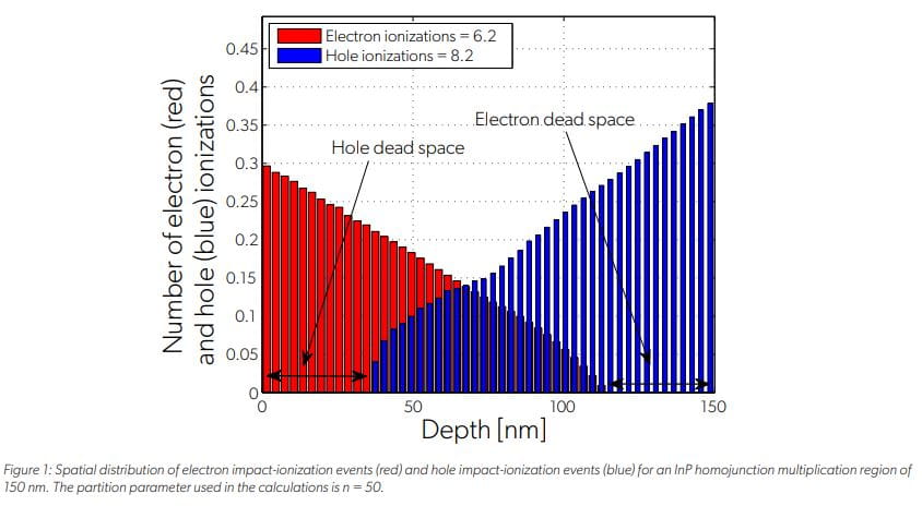
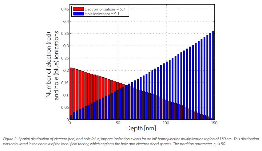
The distance at the beginning of the multiplication region—from x = 0 to x ≈ 37 nm, in which holes do not impact-ionize—corresponds to the length of the hole dead space. In this portion of the multiplication region, holes have not gained sufficient energy to initiate an impact ionization event. Similarly, the distance at the end of the multiplication region—from x ≈ 112 nm to x = 150 nm, in which electrons do not impact-ionize—corresponds to the length of the electron dead space. The calculated spatial distribution of the impact-ionization events initiated by electrons and holes are compared in Figure 2 in the context of the local-field theory, i.e., neglecting the dead space. It is clear from Figure 2 that the local-field theory does not capture the effect of the dead space on the localization of the impact-ionization events. One important implication of this result is that the local-field theory is unable to correctly predict the excess noise factor of thin multiplication regions (< 400 nm) where the dead space represents a significant portion of the multiplication region. Specifically, it is well known that the local-field theory overestimates the excess noise factor for thin APDs. For example, for the considered multiplication region operating at a mean gain of 15, the calculated excess noise factor predicted by the DSMT is approximately 5.4, yet the local-field theory predicts an excess noise factor of approximately 10.5.
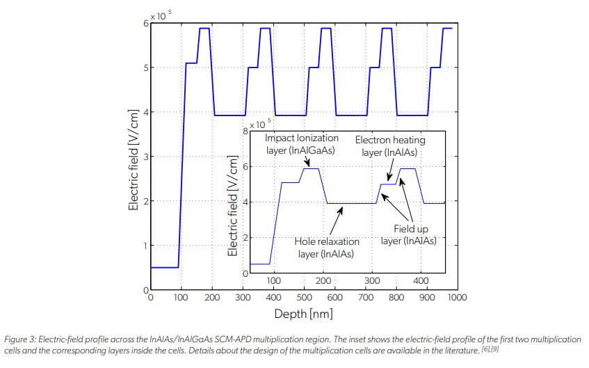
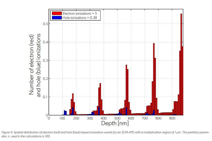
The spatial distribution of the electron and hole impact-ionization events were also calculated for a single-carrier multiplication (SCM) APD with an InAlAs/InAlGaAs multiplication region. SCM APDs were developed by the Allegro photonics group (then operating as Voxtel) to obtain quasi-deterministic multiplication gains by suppressing hole-initiated impact-ionization events. [6],[9] The multiplication region of an SCM APD consists of a cascaded multiplier architecture, which combines various design techniques to suppress hole-initiated ionizations and enhance electron-initiated ionizations. [6],[9] The electric field profile across the multiplication region is shown in Figure 3. The multiplication region has five multiplication cells, each of which consists of an avalanche layer, a hole relaxation layer, and an electron heating layer. The electric-field profile of the first two multiplications cells and the corresponding layers inside the cells are shown in the inset of Figure 3. The parent electrons are assumed to be injected at x = 0. The mechanism of hole-relaxation was modeled as described by Williams, et al. [6],[9]
The distribution of the electron and hole ionization events across the multiplication region (from Figure 3) are plotted in Figure 4. The plot shows impact-ionization events in the lower bandgap and high ionization rate layers (InAlGaAs), which are the layers where the electric field is at a maximum. The plot also shows the large difference between the number of electron impact ionizations compared and hole impact ionizations. This disparity is a result of two factors: 1) the hole-relaxation layers, which prevent the holes from acquiring sufficient kinetic energy to impact-ionize and thereby reduce excess noise; and 2) the electrons, which are pre-heated prior to injection into the InAlGaAs layer. These results are consistent with the Allegro simulation results reported by Williams, et al. [9]
Conclusion
The analytical recursive model presented here enables the distribution of electron-ionization events and hole-ionization events to be determined separately, as the avalanche process is triggered by either a parent hole or electron at an arbitrary location inside a multiplication region. The model can simulate a mechanism that suppresses the impact ionizations triggered by one species of carrier to enable determination of the effect of single carriers on localized impact ionizations. The new model is a crucial analytical tool for understanding, designing, and optimizing new generations of APDs designed to achieve ultra-low noise characteristics by enhancing impact ionizations for electrons while suppressing impact ionizations for holes (or vice versa, as may be desired).
References
[1] S. Wang, F. Ma, X. Li, R. Sidhu, X. Zheng, X. Sun, A. L. Holmes, Jr., and J. C. Campbell. Ultra-low noise avalanche photodiodes with a centered-well multiplication region. IEEE J. Quantum Electron., 39, 2003.
[2] M. M. Hayat, O-H. Kwon, S. Wang, J. C. Campbell, B. E. A. Saleh, and M. C. Teich. Boundary effects on multiplication noise in thin heterostructure avalanche photodiodes: Theory and experiment. IEEE Trans. on Electron Devices, 49(12):2114–2123, 2002.
[3] J. P. R. David and C. H. Tan, “Material considerations for avalanche photodiodes,” in IEEE Journal of Selected Topics in Quantum Electronics, 14:998– 1009, 2008.
[4] Joe C. Campbell, “Recent Advances in Telecommunications Avalanche Photodiodes,” in Journal of Lightwave Technology, 25:109–121, January 2007.
[5] W. Sun, X. Zheng, Z. Lu, and J. C. Campbell, “Monte Carlo Simulation of InAlAs/InAlGaAs Tandem Avalanche Photodiodes,” in IEEE J. of Quantum Electronics, 48:528–532.
[6] G. M. Williams, M. Compton, D. A. Ramirez, M. M. Hayat and A. S. Huntington, “Multi-Gain-Stage InGaAs Avalanche Photodiode With Enhanced Gain and Reduced Excess Noise,” in IEEE Journal of the Electron Devices Society, vol. 1, no. 2, pp. 54-65, Feb. 2013, doi: 10.1109/JEDS.2013.2258072.
[7] M. M. Hayat, B. E. A. Saleh, and M. C. Teich, “Effect of dead space on gain and noise of double-carrier multiplication avalanche photodiodes,” in IEEE Trans. Electron Devices, 39:546–552, 1992.
[8] M. M. Hayat, W. L. Sargeant, and B. E. A. Saleh, “Effect of dead space on gain and noise in Si and GaAs avalanche photodiodes,” in IEEE J. Quantum Electron., 28:1360–1365, 1992.
[9] G. M. Williams, M. Compton, D. A. Ramirez, M. M. Hayat, and A. S. Huntington, “Increased gain InGaAs avalanche photodiode with reduced excess noise achieved through asymmetric carrier modulation,” in J. Applied Physics, accepted, 2013.
This article is based on: D. A. Ramirez, M. M. Hayat, A. S. Huntington and G. M. Williams, “Non-Local Model for the Spatial Distribution of Impact Ionization Events in Avalanche Photodiodes,” in IEEE Photonics Technology Letters, vol. 26, no. 1, pp. 25-28, Jan.1, 2014, doi: 10.1109/LPT.2013.2289974. © 2014 IEEE. Personal use of this material is permitted. Permission from IEEE must be obtained for all other uses, in any current or future media, including reprinting/republishing this material for advertising or promotional purposes, creating new collective works, for resale or redistribution to servers or lists, or reuse of any copyrighted component of this work in other works.