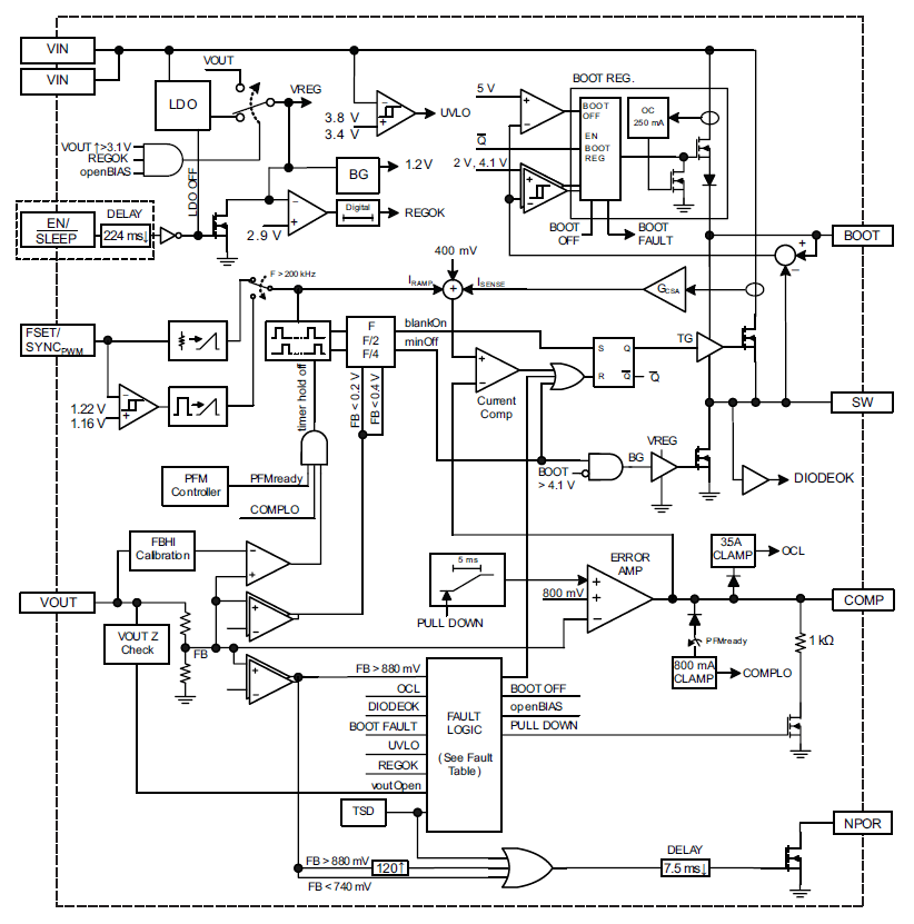
Wide Input Voltage, 2 A Buck Regulator Family with Low-IQ Mode

A8591

Product Image

Description

Top Features

Packaging

The A8591 is designed to provide the power supply requirements of next generation car audio and infotainment systems. The A8591 provides all the control and protection circuitry to produce a high-current regulator with ±1% output voltage accuracy.

The A8591 employs current-mode control to provide simple compensation, excellent stability, and fast transient response. The A8591 employs pulse-frequency modulation (PFM) to draw less than 33 μA from 12 VIN while supplying 5 V/40 μA (A8591, 5 VOUT), or less than 24 μA from 12 VIN while supplying 3.3 V/40 μA (A8591-1, 3.3 VOUT). When operational, the A8591 operates down to at least 3.6 VIN (VIN falling). The Sleep feature allows for very low standby current.

Features of the A8591 include a programmable PWM switching frequency. The regulator switching frequency can be synchronized to an external clock. The A8591 has external compensation to optimize stability and transient response for a wide range of external components and applications. The A8591 has a fixed soft-start time of 5 ms.

Extensive protection features of the A8591 include pulse-by-pulse current limit, hiccup mode short-circuit protection, open/short asynchronous diode protection, BOOT open/short voltage protection, VIN undervoltage lockout, and thermal shutdown.

The A8591 is supplied in a 10-pin wettable flank DFN package (suffix EJ) with exposed power pad. It is lead (Pb) free, with 100% matte-tin leadframe plating.

  • Automotive AEC-Q100 qualified
  • Withstands surge input to 40 VIN for load dump
  • Operates down to 3.4 VIN (typ), 3.6 VIN (max) for idle stop
  • Utilizes pulse-frequency modulation (PFM) for low-IQ mode
  • 10 μA Sleep mode (automatic PWM / Low-IQ PFM mode selection)
  • Fixed output voltage options: 3.3 or 5 V with ±1% accuracy
  • Delivers up to 2 A of output current
  • Integrated 110 mΩ high-side MOSFET
  • Adjustable switching frequency from 300 kHz to 2.4 MHz
  • EMI reduction features:
    • Frequency dithering
    • Controlled switching node
  • External synchronization capability
  • Maximum duty cycle for low dropout
  • Active low NPOR output with 7.5 ms delay
  • Pre-bias startup capable: VOUT increases monotonically, will not cause a reset
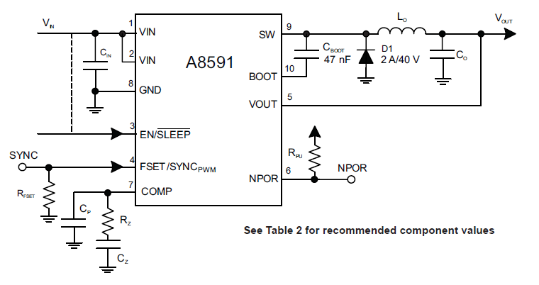
  • External compensation for maximum flexibility
  • Stable with ceramic or electrolytic output capacitors
  • Internally fixed soft-start time of 5 ms
  • Pulse-by-pulse current limit, hiccup mode short-circuit, and thermal protections
  • Pin open/short and component fault tolerant
  • –40°C to 150°C operating junction temperature range
  • Thermally enhanced DFN-10 surface-mount package

Typical Applications

Automotive:

The A8591 is supplied in a 10-pin wettable flank DFN package (suffix EJ) with exposed power pad. It is lead (Pb) free, with 100% matte-tin leadframe plating.

EJ Package Documentation

Part Number Specifications and Availability