Theory for Spatial Distribution of Impact Ionization Events in Avalanche Photodiodes
Avalanche photodiodes (APDs) are widely deployed in direct-detection, high-data rate optical fiber communication systems as well as modern lidar systems. Various approaches have been explored to reduce the excess noise of APDs, which is a measure of the uncertainty in the stochastic avalanche gain that the APD offers. These approaches include the use of thin multiplication regions [1] and impact-ionization engineered (I2E) multiplication regions. Both of these structures exploit the dead-space effect to reduce the excess noise. [2],[3] Another approach is to suppress the impact ionization of holes, β → 0, (or electrons, α → 0) to make the hole-to-electron ionization ratio, k = β/α, as disparate as possible, which would also serve to reduce the excess noise factor. As a result, there has been a growing interest in APD structures that suppress the impact ionization of one species of carrier by impact-ionization-engineering the multiplication region. [4],[5] In these structures, the suppression of the impact ionizations by one species of carrier is achieved by judiciously engineering the different layers of the heterojunction multiplication region and the electric field profile therein. A key challenge in understanding the operation of such multi-layer multiplication regions and optimizing their design is the ability to analytically determine the locations at which electrons and holes trigger impact-ionization events.
This paper reports an extension of the Dead Space Multiplication Theory (DSMT) that enables determining the spatial distribution of the impact ionizations for arbitrary heterojunction multiplication regions. The newly developed recursive equations allow determination of the number of impact-ionization events triggered by electrons and holes in an arbitrary sub-region of the multiplication region. Moreover, the model can incorporate a relaxation mechanism for suppressing the impact ionizations triggered by one species of carrier. By numerically solving an extended set of recursive equations for carrier ionizations, the spatial distribution of impact ionization has been calculated for two different cases of the multiplication region: a hole-injection InP homojunction multiplication region; and an electron-injection InAlAs/InAlGaAs I2E multiplication region. The latter structure is designed so that it suppresses the hole-initiated ionizations by incorporating a hole relaxation mechanism via phonon scattering.
The distribution across the multiplication region of the impact ionizations initiated by electrons and holes for an InP multiplication region of 1 µm under a constant electric field producing a mean avalanche gain of about 900 is shown in Figure 1. It is assumed that holes are injected at x = 0. It can be observed from the figure that the number of ionization events triggered by holes and electrons increase toward opposite ends of the multiplication region. The number of hole-initiated impact ionizations increases as the holes approach x = 1000 nm, and the number of electron-initiated impact ionizations increases as the electrons approach x = 0. This finding is consistent with the fact that holes and electrons acquire kinetic energy from the electric field traveling in opposite directions, and the number of carriers of a given type available to initiate ionization accumulates in the direction of travel.
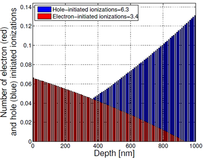
Figure 1: Spatial distribution of the impact ionization initiated by electrons (red) and holes (blue).
We have also calculated the spatial distribution of the impact ionization events considering an APD with a multi-stage InAlAs/ InAlGaAs I2E multiplication region. The electric-field profile across the multiplication region—which has five multiplication cells, each consisting of an avalanche layer, a hole relaxation layer, and an electron heating layer—is shown in Figure 2. The electric-field profile of the first two multiplications cells and the corresponding layers inside the cells is shown in the inset in Figure 2. In this multiplication region, electrons are injected at x = 0.
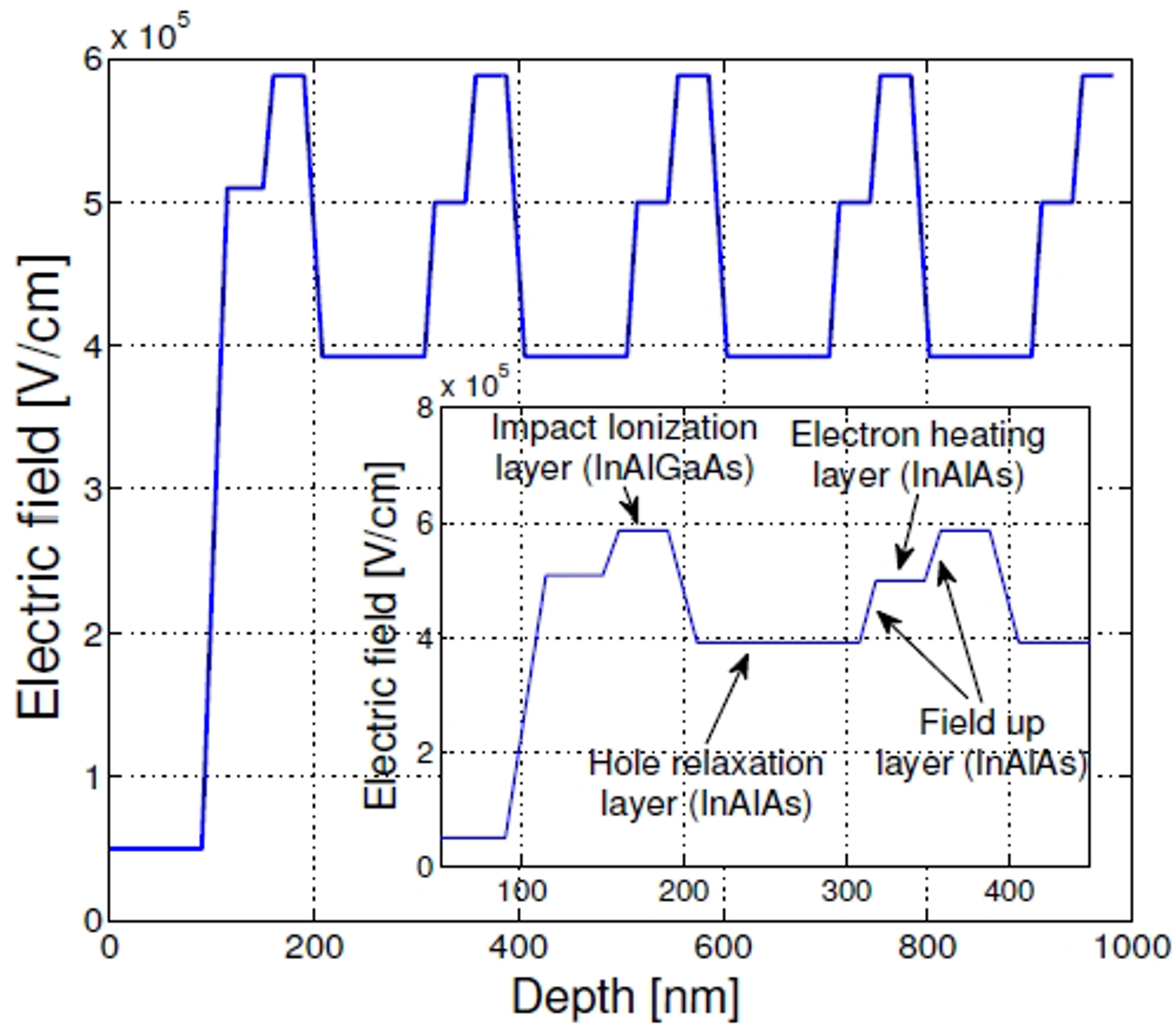
Figure 2: Electric-field profile in the I2E multiplication region.
The distribution of the impact ionizations across the multiplication region initiated by electrons and holes for the I2E multiplication region is shown in Figure 3. It can be observed from the figure that most of the impact-ionization events occur in the lower bandgap and high-ionization-rate layers (InAlGaAs), which are the layers where the electric field is at a maximum.
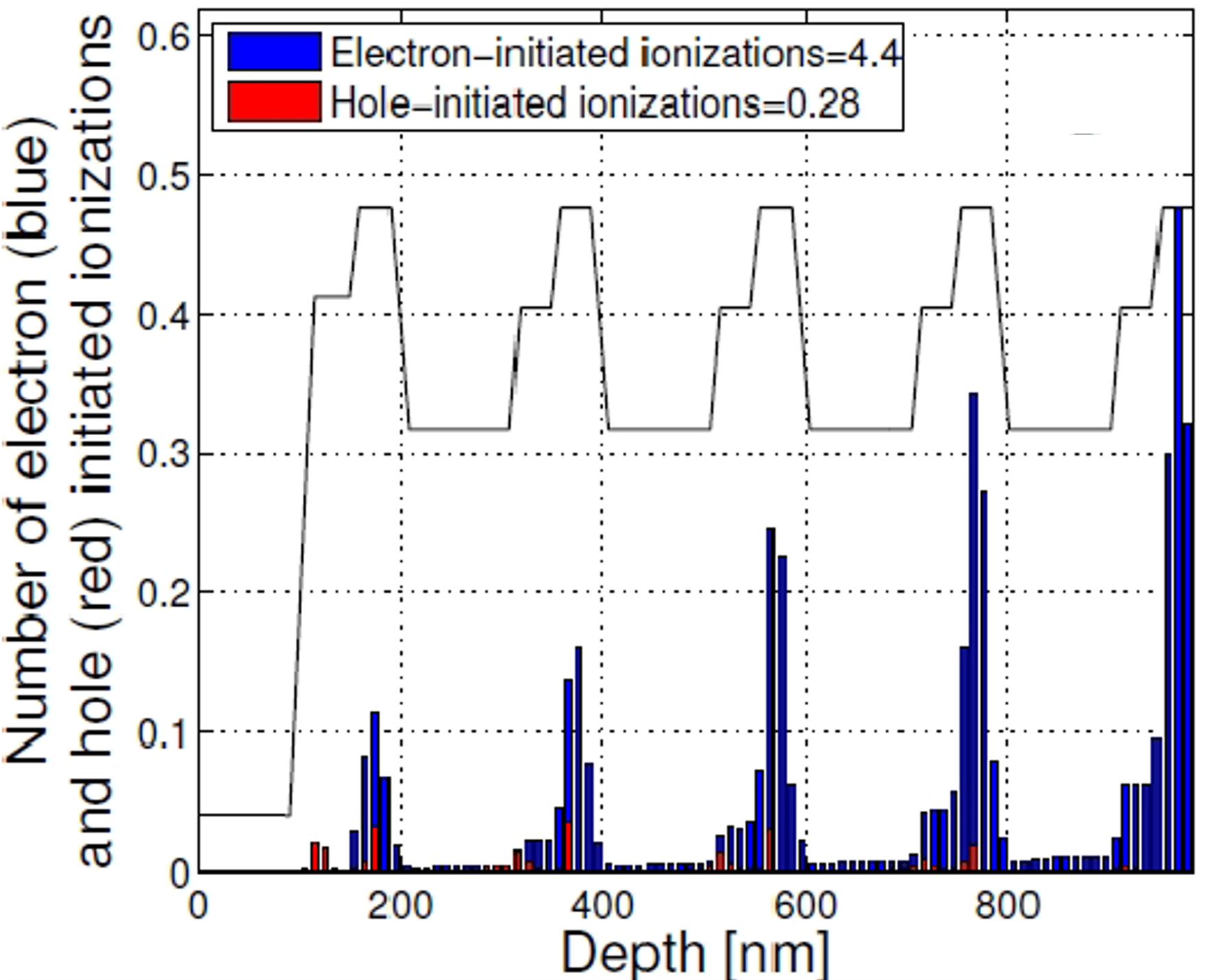
Figure 3: Spatial distribution of the impact ionization initiated by electrons (blue) and holes (red).
A magnified view of the spatial distribution of the impact ionizations is shown in Figure 4. This figure shows the large difference between the numbers of electron-initiated ionizations compared to hole-initiated ionizations. This is a result of the hole-relaxation layers, which prevent the holes from acquiring sufficient kinetic energy to impact ionize and subsequently reducing excess noise.
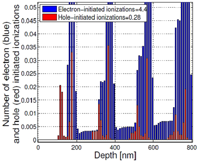
Figure 4: Magnified view of Figure 3.
In summary, we have developed an analytical recursive model to calculate the distribution of impact-ionization events triggered by holes and electrons at an arbitrary location inside the multiplication region. The model can be used to simulate a mechanism for suppressing the impact ionizations triggered by one species of carrier and to determine its effect on the distribution of impact-ionizations events.
[1] M. Hayat et al. IEEE Trans. Electron Dev., 770 – 781 (2002).
[2] S. Wang et al. IEEE J. Quantum Electron., 375 – 378 (2003).
[3] M. Hayat et al IEEE Trans. Electron Dev., 2114 – 2123 (2002).
[4] W. Sun et al. IEEE J. Quantum Electron., 528 – 532 (2012).
[5] J. Gordon et al. IEEE Electronics Letters, 519 – 519 (1979).
This article is based on: D. A. Ramirez, M. M. Hayat, A. S. Huntington and G. Williams, “Theory for spatial distribution of impact-ionization events in avalanche photodiodes,” IEEE Photonics Conference 2012, 2012, pp. 100-101, doi: 10.1109/IPCon.2012.6358508. © 2012 IEEE. Personal use of this material is permitted. Permission from IEEE must be obtained for all other uses, in any current or future media, including reprinting/republishing this material for advertising or promotional purposes, creating new collective works, for resale or redistribution to servers or lists, or reuse of any copyrighted component of this work in other works.