Reverse Battery Protection Scheme for Automotive Applications

Abstract
Many self-contained critical electronic systems and subsystems, especially in automotive applications, use a 12 V or 48 V storage battery for the primary power source. To prevent extensive damage during operational life, these systems require the design-in of systems that—at a certain voltage level—provide protection from voltage polarity reversal. This article discusses a method that provides a very low insertion loss at low cost to protect automotive systems from accidental reversal of battery polarity.
Introduction
When a system receives power from a battery that has the potential to become reverse-polarized, such as in automotive motor-driver applications, protection schemes are required that prevent reverse voltage from being applied to system components such as the gate driver, MOSFET bridge, and motor combination.
Battery polarity reversal is most likely to occur during routine servicing, battery replacement, or emergency start using an external power source.
Automotive systems that require a peak operating current of less than 10 A are usually protected by inserting a suitably rated diode in series with the power supply. For automotive systems that require higher peak and operating currents that are much higher, power MOSFET bridges can be used to drive motors.
MOSFETs used in a bridge carry most of the current supplied to the system and feature very low on-resistance, which minimizes self-heating and power loss in the motor load. Hence, a protection scheme that features very low power loss is required. Another feature of this scheme is that, if battery polarity is reversed, body diodes in each MOSFET become forward biased. If the reverse polarity voltage is greater than approximately 2 V, this condition leads to current rise limited only by the diode characteristics.
Reverse Battery Protection Circuit
A simplified block diagram of reverse battery protection systems using the charge pump voltage, VCP, to drive reverse protection circuitry is shown in Figure 1. The voltage source, VCP, is referenced to VBB and provides the gate voltage required to turn on the Q1 MOSFET. During typical operation, the Q1 MOSFET carries the full load current to the subsystem. This provides a very-low-resistance current path to minimize insertion losses when operating with typical polarity and an adequate voltage-blocking rating when battery polarity is reversed.
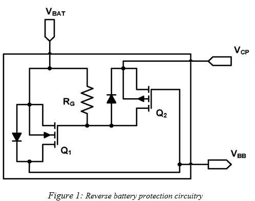
It should also be noted that the source and drain connections to the Q1 MOSFET are intentionally reversed to ensure that there is a current path through the body diode of the Q1 MOSFET, making it possible for control circuitry within the motor gate driver to start to operate during a power-up sequence. The Q2 MOSFET is a P-channel small-signal MOSFET and is used to control the gate of Q1 in correct and reverse battery conditions. Both Q1 and Q2 must be correctly rated for the full peak reverse battery voltage.
The voltage, VCP, is either produced by the gate driver itself or circuitry closely associated with it. This means that VCP is not present when VBB = 0 V, or when a reverse polarity is applied. VCP also takes some time to rise to a final stable value after VBB is applied. From the VCP supplies, resistor RG—with minimum value of 100 kΩ ±1%—controls the gate-to-source voltage of Q1.
Circuit Operation With VCP
Correct Battery Polarity
The position of impedance ZL is shown in Figure 2. ZL provides a current path from VBB to ground via the power bridge and the motor under all conditions.
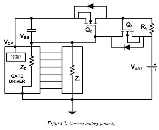
The sequence of events during start-up is:
- With VBAT = 0 V, current does not flow in ZD and ZL, and VCP = 0 V.
- VBAT, with the correct polarity, is applied to the gate driver.
- Current flows through the forward-biased body diode of Q1 and the gate driver, causing it to execute a power-on-reset cycle and initialize.
- As the gate driver progresses through its various control states, it causes the value of VCP referenced to VBB to increase from zero and to raise the voltage on the source of Q2, such that it becomes more positive than VBB. This action increases the gate-to-source voltage on Q2.
- As VCP rises above the conduction threshold of Q2, it starts to turn on, and current flowing through it produces a voltage across the RG resistor. This voltage appears across the gate and source of Q1, and it also starts to turn on.
- As Q1 starts to conduct, the main supply current from VBAT is shared between its body diode and source-to-drain path.
- At sufficiently high values of VCP, the on-resistance of Q1 becomes sufficiently low that the source-to-drain voltage falls below the forward voltage of the body diode in Q1, and conduction ceases. All current then flows between the source and drain of Q1 to produce an insertion loss.
Reverse Battery Polarity
The reverse battery polarity condition is shown in Figure 3. In this condition, VCP is always 0 V because the gate driver never achieves an operating condition.
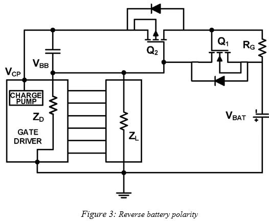
The sequence of events during start-up is:
- As VBAT increases in a negative direction, the 0 V VGS condition persists on the gates of Q1 and Q2, and both transistors remain turned off.
- Because Q1 and Q2 remain turned off, all applied reverse voltage appears across the source and drain connections of Q1 and Q2. As a result, voltage across the gate driver and ZL remain at 0 V.
- When VBAT is in the reverse polarity condition, current does not flow through the gate driver.
- This condition is stable until the source-to-drain voltage breakdown rating of either Q1 or Q2 is exceeded by the reverse voltage on VBAT.
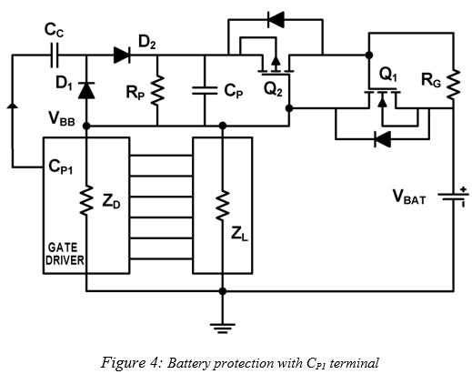
Circuit Operation with Internal Charge Pump
Many products feature an output from an internal regulator charge pump that runs and switches continuously. The signal of the internal regulator charge pump, CP1, may be used to pump a circuit that creates a voltage supply equivalent to the VCP presented in Figure 1, Figure 2, and Figure 3. Operation of the circuit, as illustrated in Figure 4 under both correct and reverse voltage polarity conditions, closely follows the earlier description in the Circuit Operation with VCP section.
Circuit Operation with Bootstrap Capacitor
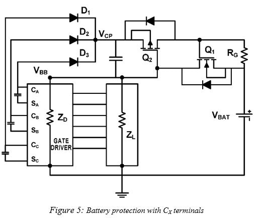
Some products have neither an internal charge pump to provide the VCP voltage nor an internal regulator charge pump to provide continuous running and switching. Instead, they use bootstrap capacitors to create the gate voltage required by the high-side power MOSFETs in the main output power bridge. Bootstrap capacitors are connected between bootstrap supply terminals CA, CB, and CC and corresponding reference pins SA, SB, and SC, as shown in Figure 5. When the system operates with a positive polarity on VBAT, the operation of the bootstrap capacitors, CBOOTA, CBOOTB and CBOOTC, typically results in the voltage on the CA, CB, and CC terminals of the gate driver switching higher than the VBB voltage when any high-side driver in the power bridge is commanded to turn on. Diodes D1, D2, and D3 (see Figure 5) ensure that the peak voltage from any of the CA, CB, and CC terminals is delivered to the source of the Q2 MOSFET, as presented in Figure 5. The Q2 MOSFET operates as a typical on-switch, unless the voltage on terminals CA, CB, and CC is kept below the turn-on threshold of the Q2 MOSFET. Therefore, the peak voltage from CA, CB, or CC is applied to the gate of the Q1 MOSFET. The gate-to-source capacitance of the Q1 MOSFET can store charge from the bootstrap capacitors and produce a DC voltage for the gate of the Q1 MOSFET. Using the scheme described here, a voltage supply equivalent to the VCP voltage presented in Figure 1 has been created. Operation of the circuit, as illustrated in Figure 5 under the correct and reverse voltage polarity conditions, closely follows the earlier description in the Circuit Operation with VCP section.
Experimental Results
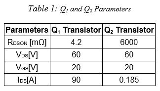
The performance of the reverse battery protection circuit presented in Figure 1 was experimentally verified on the bench. Several experiments were performed on the bench using an Allegro AMT49107 gate driver, which has an internally designed charge pump terminal, VCP. The test bench contains a dual DC power supply, commercially available 1 GHz scope, and Allegro AMT49107 demonstration board, which has a built-in reverse battery protection circuit. The parameters of the Q1 and Q2 transistors employed are presented in Table 1.
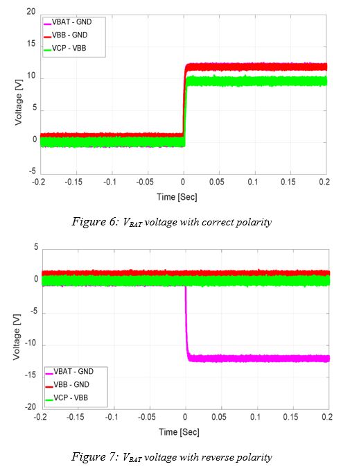
Experimental tests were performed by applying stepped voltage changes—from 0 V to 12 V and 0 V to –12 V—on the battery under test and observing the performance of the reverse battery protection circuit by monitoring the VBAT, VBB, and VCP signals, as presented in Figure 6 and Figure 7. The performance of the reverse battery protection with the correct polarity is shown in Figure 6: During power-up, the initial system current is supplied to VBB through the forward-biased source-to-drain diode of transistor Q1 until VCP voltage exceeds the threshold voltage of Q1 and turns it on. The behavior of the reverse battery circuit with reverse polarity is shown in Figure 7: When the battery voltage is reversed, the voltage between VCP and VBB is zero, the gate-to-source voltage on Q1 is zero, and its source-to-drain diode becomes reverse biased. In this condition, Q1 blocks current flow to VBB, and the voltage between VBB and ground remains at approximately 0 V.
Summary
The reverse battery protection schemes described in this article can be used with Allegro gate drivers for automotive applications that employ gate drivers that have an internal charge pump terminal or an internal regulator charge pump terminal, or that use bootstrap capacitors.
A list of the most prevalent Allegro gate drivers in automotive applications is provided in Table 2 along with the corresponding reverse battery protection techniques described in this article. Experimental results demonstrate that these gate drivers can be protected against the reverse battery polarity that can occur by changing the battery of a vehicle or during routine maintenance work on electronic systems.
Table 2: Allegro Gate Drivers and Reverse Battery Protection
|
Gate Driver |
VCP |
CP1 |
Bootstrap |
|
No |
Yes |
Yes |
|
|
No |
No |
Yes |
|
|
No |
No |
Yes |
|
|
No |
Yes |
Yes |
|
|
No |
No |
Yes |
|
|
No |
No |
Yes |
|
|
No |
No |
Yes |
|
|
No |
No |
Yes |
|
|
No |
No |
Yes |
|
|
No |
No |
Yes |
|
|
No |
No |
Yes |
|
|
Yes |
No |
Yes |
|
|
Yes |
No |
Yes |
|
|
Yes |
No |
No |
|
|
Yes |
No |
No |
Based on the article, "Reverse battery protection scheme for automotive applications" by Dr. Kavul Tshiloz, originally published in Electronics Specifier, April 18th, 2023. Republished with permission. For portions not copyrighted by original publisher, Copyright ©2023, Allegro MicroSystems, Inc.
Copyright 2023, Allegro Microsystems.
The information contained in this document does not constitute any representation, warranty, assurance, guaranty, or inducement by Allegro to the customer with respect to the subject matter of this document. The information being provided does not guarantee that a process based on this information will be reliable, or that Allegro has explored all of the possible failure modes. It is the customer's responsibility to do sufficient qualification testing of the final product to ensure that it is reliable and meets all design requirements.
Copies of this document are considered uncontrolled documents.