ACS712 and ACS713 Current Sensor ICs Frequently Asked Questions

Allegro® MicroSystems current sensor ICs are isolation-tested according to the IEC 60950 standard. The ACS714 and ACS715 devices have a 2100 VRMS rating for reinforced isolation and a 1500 VRMS rating for basic isolation. For reinforced insulation, this allows for a working voltage of up to 184 Vpeak or DC voltage. This allows for use on 110 VAC mains for reinforced applications. For basic isolation this translates to a working voltage of 354 Vpeak or DC voltage. This is suitable for use on 240 VAC circuits.
Basic isolation voltage refers to isolation ratings for circuitry connected between line voltage and ground. Reinforced isolation voltage refers to isolation ratings for circuitry connected between line voltage and secondary electrical equipment that may have user contact. The following figure compares these specifications.

 isolation

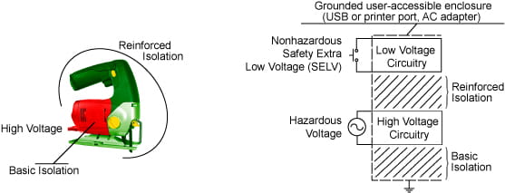
For the ACS712 and ACS713, the key limitation is actually the creepage and clearance distance inherent in the SOIC8 package. To achieve higher isolation voltage ratings, steps must be taken in the applications themselves, such as adding a slit on the circuit board underneath the device to increase the creepage distance, and possibly adding a conformal coating to increase the clearance distance. Because these solutions are a function of the PCB layout and the coating compound used, if a safety isolation standard is to be met, it must be certified at the application level.

The ACS712 and ACS713 use Hall effect technology, which is compatible with electrical currents having both DC and AC components. The bandwidths are 80 kHz typical.
The ratiometric feature of the ACS712 and ACS713 means the device gain and offsets are proportional to the supply voltage, VCC. This feature is particularly valuable when using the ACS712 and ACS713 with an analog-to-digital converter. A-to-D converters typically derive their LSB from a reference voltage input, and if the reference voltage varies, then the LSB varies proportionally. If the reference voltage and the supply voltage for the ACS712 and ACS713 are derived from the same voltage source, then both the ACS712 and ACS713 outputs and the A-to-D converter LSB track any variations in the reference voltage source. Therefore, reference voltage variations will not be a source of error in the analog-to-digital conversion of the ACS712 and ACS713 output signals. Figure 2 is a plot of primary current, IP, versus output voltage, VOUT, of the ACS712ELC-20A-T when varying VCC. The offset and sensitivity levels shift proportionally with VCC. For example, when VCC = 5.5 V, the 0 A output is 5.5 / 2 = 2.75 V nominal, and the sensitivity is 110 mV/A nominal.
 
 figure 2
Figure 2. ACS712ELC-20A-T Characteristic Performance: VOUT versus IP at Various VCC Levels. 
Allegro recommends the use of a 0.1 µF bypass capacitor between the VCC pin and the GND pin. The capacitor should be located as close as practical to the ACS712 and ACS713 package body.
No, the ACS712 and ACS713 mV/A sensitivity and 0-ampere quiescent voltage level are programmed by Allegro.
The resolution of the ACS712 is limited by its noise level. The filtering characteristics are provided in table 1.

Table 1. ACS712ELC-05B Noise Level and Resolution
versus Filtering Capacitance and Resulting Bandwidth

Sens = 185 (mV/A)

Pk-Pk Noise
(mV)

Current Resolution
(mA)

Cf
(nF)

BW
(kHz)

92

497

0

80

46

249

4.7

19.9

26

141

22

4.3

20

108

47

2.0


If higher resolution is required, then please contact the Allegro factory. Allegro continues to innovate and improve upon the industry leading noise performance of our current sensor ICs. We are likely to have a higher resolution product in our portfolio that may meet the needs of your application.

Typical ESD tolerance is 6 kV human body model, 600 V machine model.
Yes, download from: Gerber Files (ZIP).
Yes, a bill of materials from: ACS712 Bill-of-Materials (PDF). 
The clearance distance, distance through air between the primary leads and secondary leads, for the ACS712 is typically 2 mm. This is the shortest distance from the primary leads to the tie-bar on the side of the package, which is connected to the secondary leads (see figure 3). The clearance distance can be increased by adding a conformal coating.
 
 
Figure 3. ACS712 lead-frame. The clearance distance is shown to be approximately 2 mm.

The creepage distance on the surface of the device package is also approximately 2 mm, as, again, the shortest distance from the primary to the secondary leads is along the edge of the package to the tie-bar on the side of the package.
The creepage distance on the surface of the printed circuit board on which the package is mounted is approximately 3.9 mm. However, this may be increased, if necessary, by cutting a slit on the board between the solder pads on opposite sides of the package (see figure 4).
 
Figure 4. Typical slit cut into the PCB underneath the package, 
separating the two banks of pins, to further control creepage. 
Typical measured inductance versus test signal frequency:
  • 2.5 nH at 10 kHz 
  • 2.4 nH at 50 kHz 
  • 2.2 nH at 100 kHz 
  • 2.15 nH at 200 kHz 
The value is extremely small and was measured to be less than 1  pF (typical).
The evaluation board uses 2-oz. copper.
Care should be taken to minimize the inductance of the current path to be measured. Also, attention should be paid to minimizing the contact/connection resistance of any connections in that path.
The leadframes of the ACS712 and ACS713 are plated with lead-free, 100% matte tin and hence should be processed and soldered accordingly. However the ACS712 and ACS713 are flip-chip devices, and the solder balls inside the package that connect the die to the leadframe are 95% lead, 5% tin. Lead-free alternatives for high-temperature flip-chip solder balls are not yet commercially available, and therefore solder balls of this composition are exempted from lead-free requirements of RoHS (Directive 2002/95/EC of the European Parliament and of the Council of 27 January 2003 on the Restriction of the Use of Certain Hazardous Substances in Electrical and Electronic Equipment).
The leadframe is made of oxygen-free copper.
Assumptions for subsequent analysis:
A. The stray field results from a current flowing through a printed circuit board (PCB) trace , or an external current-carrying conductor, adjacent to the Allegro device.
B. The external current-carrying conductor is on the same plane as the Hall element.
C. The conductor has an infinite length.
The assumptions above provide a worst case analysis for stray field generated by the current-carrying conductor because there is no shielding of the Hall element, and the Hall element is in the optimum plane relative to the disturbance.
The magnetic field, B, generated in the direction perpendicular to the plane in which the conductor and the Hall element lie, at the distance λ to the conductor, will be:
BEXT = μ0  × I / ( 2 π × λ )  (tesla),
where:
   μ0 = 4 π×10E-7  (H/m),
        = 400 π  (nH/m), and
        assuming no core material around;
   I is in amperes, and is the magnitude of the current flowing in the conductor; and 
   λ is in meters, and is the distance between the point under consideration and the conductor.
The analysis is based on the fact that the magnetic coupling coefficient of ACS712 family is typically 12  gauss/A.
The percentage error on the ACS712 output signal that is purely a result of an external magnetic disturbance (percentage is relative to the full scale current range of the device) can be calculated as:
 
Error from External Field = ( BEXT / [12 G / A × IP ] ) × 100  (%). 
Figure 5 shows the absolute current error (in A) versus the distance of the Hall element from the primary conductor (in mm) for different primary current values (in A).


figure 4
Figure 5. Absolute Output Signal Error versus Distance between the 
Hall Element and an External PCB Conductor at Various Current Levels. 
The ACS712 and ACS713 also have been certified by TÜV America to the following standards:
  • UL 60950-1:2003 
  • EN 60950-1:2001 
  • CAN/CSA C22.2 No. 60950-1:2003 
The mold compound is UL recognized to UL94V-0. 
The output may become unstable and oscillate.
The output may not be able to fully drive the load and therefore it may not be as accurate as the datasheet specification. If the output resistance becomes very low, or is shorted to VCC, the output may be permanently damaged if the overload current continues for a period of time.
Steady state thermal testing with continuous DC (or AC RMS) current, based on Allegros ASEK712 demo board, shows that at an ambient temperature of 85°C the ACS712 can withstand a maximum of 40 A before reaching the maximum thermal junction temperature of 165°C. If the ambient temperature is as high as 150°C, the ACS712 can withstand up to a maximum of 20 A before reaching a junction temperature of 165°C. See figure 6.
figure 5 
Figure 6. Typical ACS712 Die Temperature versus Continuous DC IP Current 

In the case of higher value current pulses with small duty cycles, please see table 2.

Table 2. ACS712 Sustainable Pulsed DC Primary Current Rates*

Current Amplitude
(A)

Pulse Duration
(ms)

Duty Cycle
(%)

Maximum Quantity
of Pulses Allowed

60

1000

10

Unlimited

120

20

10

Unlimited

200

10

10

10

200

10

1

Unlimited

100

10

10

Unlimited

*The data in this table is valid at TA=25°C only, and was taken using the Allegro ASEK712 demo board.


Test results, based on limited samples, are shown in table 3.

Table 3. Typical Leadframe Resistance at Various Ambient Temperatures

TA
(°C)

Leadframe Resistance
(mΩ)

Quantity
of Samples

Max

Mean

Min

-40

1.25

0.8

0.46

82

25

1.39

1.03

0.47

85

85

1.46

1.09

0.53

79

150

1.61

1.28

0.91

87 

The ACS712 family of devices will operate, on average, well above the rated working voltage in the datasheet. However, mostly because of safety certification compliance requirements, Allegro does not approve of or recommend use of the device beyond the voltage ratings specified in the device datasheets. If you have a need for a device with higher voltage isolation performance, then please contact the Allegro factory.