Have Questions? Let us help!
We're passionate about innovation. Reach out and you'll hear back from an expert shortly.
One of our solution experts will be in touch with you shortly. Keep reading to learn more about our industry leading solutions.
Allegro® MicroSystems current sensor ICs are isolation-tested according to the IEC 60950 standard. The ACS714 and ACS715 devices have a 2100 VRMS rating for reinforced isolation and a 1500 VRMS rating for basic isolation. For reinforced insulation, this allows for a working voltage of up to 184 Vpeak or DC voltage. This allows for use on 110 VAC mains for reinforced applications. For basic isolation this translates to a working voltage of 354 Vpeak or DC voltage. This is suitable for use on 240 VAC circuits.
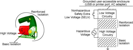
Basic isolation voltage refers to isolation ratings for circuitry connected between line voltage and ground. Reinforced isolation voltage refers to isolation ratings for circuitry connected between line voltage and secondary electrical equipment that may have user contact. The following figure compares these specifications.
For the ACS714 and ACS715, the key limitation is actually the creepage and clearance distance inherent in the SOIC8 package. To achieve higher isolation voltage ratings, steps must be taken in the applications themselves, such as adding a slit on the circuit board underneath the device to increase the creepage distance, and possibly adding a conformal coating to increase the clearance distance. Because these solutions are a function of the PCB layout and the coating compound used, if a safety isolation standard is to be met, it must be certified at the application level.
Can the ACS714 and ACS715 be applied to both DC and AC currents?
The ACS714 and ACS715 use Hall effect technology, which is compatible with electrical currents having both DC and AC components. The bandwidths are 80 kHz typical.
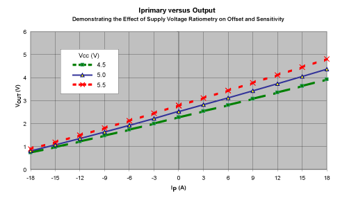
The ratiometric feature of the ACS714 and ACS715 means the device gain and offsets are proportional to the supply voltage, VCC. This feature is particularly valuable when using the ACS714 and ACS715 with an analog-to-digital converter. A-to-D converters typically derive a reference voltage from the A/D VCC voltage rail input. If the A/D VCC voltage varies, then the reference varies proportionally. One advantage of ratiometry is, if the reference voltage and the supply voltage for the ACS714 and ACS715 are derived from the same source, then both the ACS714 and ACS715 and the A-to-D converter track those variations, and such variations will not be a source of error in the analog-to-digital conversion of the ACS714 and ACS715 output. Below is a plot of primary current, IP, to output voltage, VOUT, of the ACS714 and ACS715 when varying VCC. The offset and sensitivity levels shift proportionally with VCC. For example, when VCC = 5.5 V, the 0 A output is 5.5 / 2 = 2.75 V nominal, and the sensitivity is 110 mV/A nominal.
What external components are required?
Allegro recommends the use of a 0.1 µF bypass capacitor between the VCC pin and the GND pin. The capacitor should be located as close as practical to the ACS714 and ACS715 package body.
Is there any way to adjust the gain of the ACS714 and ACS715?
No, the ACS714 and ACS715 mV/A sensitivity and 0-ampere quiescent voltage level are programmed at the factory.
Do the ACS714 and ACS715 contain lead?
The leadframes of the ACS714 and ACS715 are plated with lead-free, 100% matte tin and hence should be processed and soldered accordingly. However the ACS714 and ACS715 are flip-chip devices, and the solder balls inside the package that connect the die to the leadframe are 95% lead, 5% tin. Lead-free alternatives for high-temperature flip-chip solder balls are not yet commercially available, and therefore solder balls of this composition are exempted from lead-free requirements of RoHS (Directive 2002/95/EC of the European Parliament and of the Council of 27 January 2003 on the Restriction of the Use of Certain Hazardous Substances in Electrical and Electronic Equipment).
What is the composition of the leadframe?
The leadframe is made of oxygen-free copper.
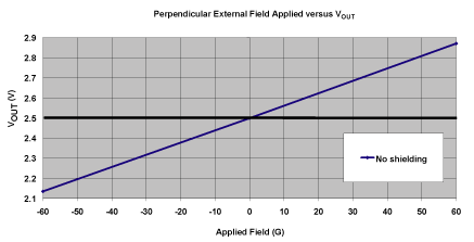
How susceptible is the ACS714 and ACS715 to stray magnetic fields?
The magnetic coupling of the ACS714 and ACS715 is listed in the datasheets with a nominal value of 12 G/A. What this means is, for every ampere of current, 12 G of field is produced at the Hall element. For stray fields, the effect on the device can be calculated by dividing 12 G/A by the mV/A sensitivity of the device in use. This allows you to predict the Gauss per millivolt change at the output. The susceptibility of the ACS714 and ACS715 to external fields can be mitigated via proper orientation, spacing from external field sources, and if necessary, shielding of the device. An application note, Managing External Magnetic Field Interference When Using ACS70x and ACS71x Current Sensor ICs (PDF) addresses mitigation techniques in greater detail.
What safety certifications do the ACS714 and ACS715 have?
The ACS714 and ACS715 also have been certified by TÜV America to the following standards:
What are the creepage and clearance distances between the current path and the signal circuit?
The clearance distance, distance through air between the primary leads and secondary leads, for the ACS714 and ACS715 is typically 2 mm. This is the shortest distance from the primary leads to the tie-bar on the side of the package, which is connected to the secondary leads (see figure below). The clearance distance can be increased by adding a conformal coating.
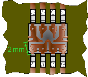
ACS714 amd ACS715 leadframe. The clearance distance is shown
to be approximately 2 mm.
The creepage distance on the surface of the device package is also approximately 2 mm, as, again, the shortest distance from the primary to the secondary leads is along the edge of the package to the tie-bar on the side of the package.
The creepage distance on the surface of the printed circuit board on which the package is mounted is approximately 3.9 mm. However, this may be increased, if necessary, by cutting a slit on the board between the solder pads on opposite sides of the package (see figure below).
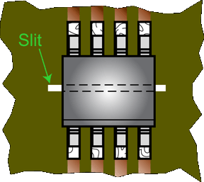
Typical slit cut into the PCB underneath the package,
separating the two banks of pins, to further control creepage.