Solving Gate Drive Challenges with Technology for Improved Power Design
Introduction
With an increased global focus on clean electricity generation, storage, and consumption across many applications, the need for better power conversion modules is exploding. Engineers and designers in the automotive, industrial, cloud computing, and clean energy sectors are seeking ways to get more electricity from conversions in the smallest possible footprint.
Great strides in technology have been made in these areas, and engineering teams are now embracing new power switch technologies such as wide bandgap Silicon Carbide (SiC), Field Effect Transistors (FET), and Gallium Nitride (GaN) FETs - which deliver significant benefits in terms of efficiency and power-density for power conversion modules compared to the traditional switching methods (MOSFETs, IGBTs, etc.).
Challenges
Designing power modules always comes with multiple challenges and tradeoffs, many of which are related to the driving of these FETs, particularly when for safety reasons, an electrical isolation barrier is required in the system (to protect both user and the lower voltage parts of the system). These challenges include:
1. The need for additional bootstraps circuits & capacitors – these are additional components that need to carefully be chosen and dimensioned in a balancing act of tradeoffs between system power efficiency, isolation efficiency, voltage stresses on components and switching frequency
2. Multiple power rails circuit designs that pose challenges in terms of power integrity, efficiency, sequencing, and fault managements while increasing electromagnetic interface (EMI). Indeed, the use of any power supply adds stray capacitance in the system. For a switch located in the high side of a full bridge, the additional stray capacitance is likely to create common-mode and electromagnetic interference, which brings new design challenges. Also, stray capacitance can allow for the flow of high-voltage current spikes, which can interfere with correct functional operation. These issues are likely to occur even if the power device is driven across an isolation barrier EMI – requiring bulky, not easy to design filters
These challenges lead to increased component counts, volume, and system design complexity. Although the new switch technologies allow to deliver significant benefits, they do make above driving challenges even more complex to solve, thus lengthening design cycles and preventing designers from leveraging the full capabilities of these new wide band gap FETs with traditional FET driving solution. An easier design process would be to use a gate driver that also supplies the power needed to control the switches and a single capacitor to create the floating voltage for the high-side switches.
Solution
While significant advancements in switching technologies have been made in the past decade with the introduction of wide band gap switches, significantly equivalent advancements required in the driving of these switches have remained surprisingly absent. Usual gate driving technologies still rely on the novelties from the 1970s. It is no lack of R&D efforts at cause (although much more R&D went into switching), but rather the complexity of finding a simpler and more efficient way to get power across the isolation barrier.
That was until Allegro developed groundbreaking Power-Thru technology: a long-awaited solution that eliminates the need for external power supplies and bootstrap circuitry.
In a minimal single package design that eliminates bulk from the PCB, Power-Thru technology uses a novel magnetic coupling device that simultaneously transfers the gate on/off logic signal, and delivers the power needed to drive the gate of the switch across the isolation barrier. The full electrical isolation provided by their magnetic coupling makes Power-Thru gate drivers ideal for use in high-side, low-side, and isolated applications alike.

Figure 1: A complete regular gate drive circuit (inside the red shape) with multiple components on the left, is replaced by a single package offering all the required functionalities to optimally drive a switch.
Benefits
Eliminating bootstrap circuits and bias supply come with the Power-Thru technology generates noticeable typical benefits, such as 50% reduction of components, allowing for a doubling of the power-density and elimination of the complexity of the gate driving design, resulting in half the required design time.
But the Power-Thru technology offers even more benefits. By eliminating the bias supply, the total gate driving common mode capacitance of the system is less than 1 pF, while this value is around 11 pF for comparable system with bias supply. This reduction of 10 pF offers significant benefits:
- Less power dissipation because much less Common Mode capacitance needs to be charged/discharged every PWM cycle
- Less current spikes in the system
- Less voltage spikes
- Significant reduction in EMI, typically more than 20 dB. This allows for much smaller EMI filters, thus again saving on system component costs and size
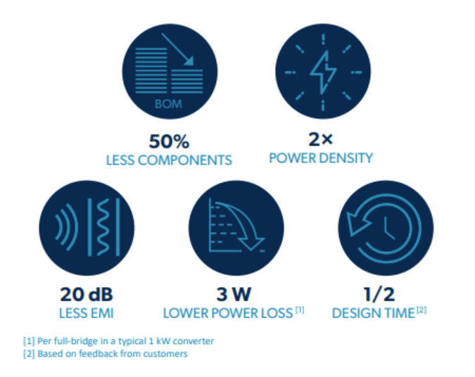
Figure 2: Typical benefits achieved with the AHV85110 and AHV85111, the first isolated gate driver with Power-Thru technology launched to the market. New gate drivers with Power-Thru technology will be released regularly to cover all switching technologies. Energy loss in a typical 1kW full-bridge converter, design time reduction reported by customers.
Conclusion
Allegro’s isolated gate drivers with Power-Thru technology allows the removal of traditional design challenges and trade-offs in terms of driving switches in high-voltage circuits. This subsequently unlocks the full potential of wide bandgap switches with new levels of power-density and efficiency, while significantly reducing BOM count, complexity, EMI noise, design cycle and system cost. A game changer.
Based on the article, "How Power-Thru Technology Enables Improved Power Modules" by Bernard Gouverneur, originally published in Semiconductor Digest. Republished with permission. For portions not copyrighted by original publisher, Copyright ©2024, Allegro MicroSystems, Inc.
Copyright 2024, Allegro Microsystems.
The information contained in this document does not constitute any representation, warranty, assurance, guaranty, or inducement by Allegro to the customer with respect to the subject matter of this document. The information being provided does not guarantee that a process based on this information will be reliable, or that Allegro has explored all of the possible failure modes. It is the customer's responsibility to do sufficient qualification testing of the final product to ensure that it is reliable and meets all design requirements.
Copies of this document are considered uncontrolled documents.