Isolated Gate Drivers
Self-Powered Isolated GaN FET Driver with Integrated Bias Supply
AHV85110
Markets Served
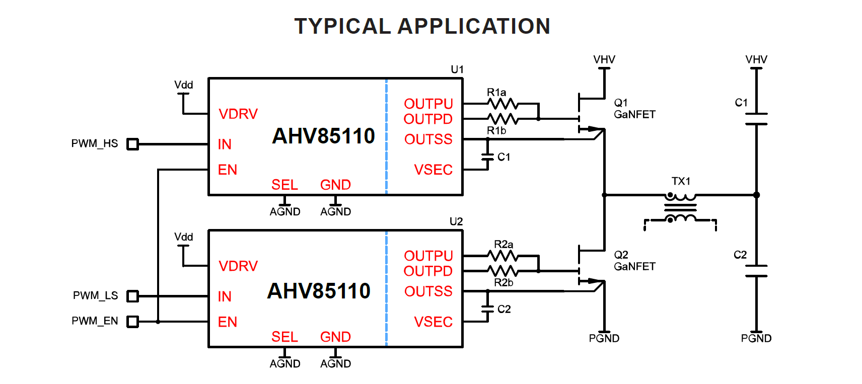
The AHV85110 simplifies isolated gate drive designs for GaN FETs, with an integrated bias supply that eliminates the need for external components. Offers high dv/dt immunity, fast propagation delay, and robust protection features.
Product Details
Product Details
Top Features
- Transformer isolation barrier
- Power-Thru integrated isolated bias
- No need for high-side bootstrap
- No need for external secondary-side bias
- AEC-Q100 Grade 2 qualification
- 50 ns propagation delay
Target Application
- DC-DC Converter
- Auxilary Inverter
- On-board Charger
- Server Power
- C&I Solar String Inverters

Part Number Specifications and Availability
HV Isolated Evaluation Boards
| EVK PN | Switch | Supplier / PN | Description | Gate Driver Used | |
|---|---|---|---|---|---|
| APEK85110KNH-01-T-MH Evaluation Board User Guide (GaN Systems FETs) | E-Mode GaN | GaN Systems GS66516B | Half-bridge bipolar driver-switch board | AHV85110 | Buy Now |
| APEK85110KNH-05-T-MH Evaluation Board User Guide (Nexperia FETs) | E-Mode GaN | Nexperia GAN080-650EBE | Half-bridge bipolar driver-switch board | AHV85110 | Buy Now |
| APEK85110KNH-06-T Evaluation Board User Guide (Transphorm FETs) | GaN | Transphorm TP65H070G4QS | Half-bridge bipolar driver-switch board | AHV85110 | Buy Now |
AHV85110 Product Video
The AHV85110 isolated gate driver is optimized for driving GaNFETs in multiple applications and topologies. An isolated output bias supply is integrated into the driver device, eliminating the need for any external gate drive auxiliary bias supply or high-side bootstrap. This greatly simplifies the system design and reduces EMI through reduced total common-mode (CM) capacitance. It also allows the driving of a floating switch in any location in a switching power topology.
0:00

Technical Documentation

Application Note
Design and Application Guide for AHV85110
Application Note
Minimizing PCB Parasitic Effects with Optimum Layout of the Gate Driver Loop Applicable to AHV85110 AND AHV85111 Gate Drivers
Application Note
FET Gate Drive and Bipolar Output Applicable to AHV85110KNHTR Gate Drivers
Blog
Powering the Next Generation of High-Density GaN Modules: Allegro MicroSystems + RAM Innovations

Brochure
Efficient Climate Control, Engineered to Perfection - Driving Performance and Sustainability in Next-Generation Heat Pumps and HVAC Systems New
Brochure
Electrifying the Open Road - Unleashing Performance and Reliability in Electric Motorcycles New
Brochure
Empowering the Renewable Grid - Driving Efficiency, Reliability, and Density in Solar String Inverters
Brochure
Robust and Efficient UPS Solutions Powered by Allegro
Brochure
Robust and Efficient Power Supply Units (PSUs) for Cloud Infrastructure
Brochure
Precision in Motion: Powering the Future of Collaborative Robotics
Brochure
DC Fast Charging: Faster and Farther
Brochure
Comfort Through Sustainability - Unlock the Power of Heat Pump Innovation
Brochure
xEV Thermal Management System Brochure
Brochure
Brochure: The AHV85110 Overview
Brochure
Brochure: Solar Energy Harvesting

Guide
APEK85110KNH-05-T-MH Evaluation Board User Guide (Nexperia FETs)
Guide
APEK85110KNH-01-T-MH Evaluation Board User Guide (GaN Systems FETs)
Guide
APEK85110KNH-06-T Evaluation Board User Guide (Transphorm FETs)
Guide
AHV85110 Simplis Modeling Guide

Infographic
Power-Thru-Technology Infographic

Technical Article
Solving Gate Drive Challenges with Technology for Improved Power Design
Technical Article
Solving the Challenges of Increasing Power Density by Reducing Number of Power Rails
Technical Article